
19D YUANDEAN
Document overview
- Manufacturer or author: Provided By www.digicamel.com(FREE DATASHEET DOWNLOAD SITE)
- PDF pages: 2
Technical content
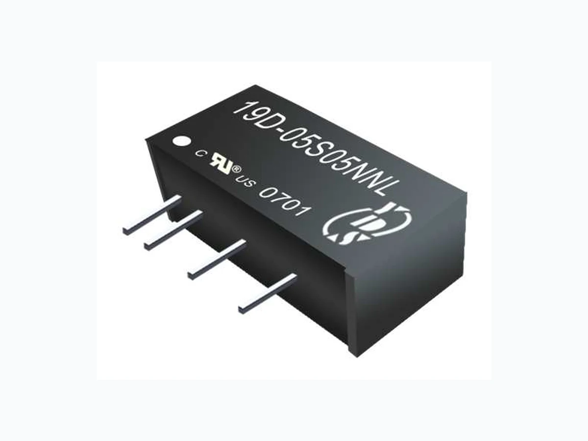
FEATURES : 7PIN SIP PACKAGE High Efficiency up to 85% Single Output 5/9/12/15V/24V Approved By UL60950-1 Unregulated Output Types Internal SMD Construction No External Component Required Operating Temperature:-40℃ TO +85℃ Industry Standard Pinout DC-DC Converter 19D SERIES 2Watt 1KV Isolated Single & Dual Output SIP7 Specifications typical at TA=25°C, nominal input voltage and rated output current unless otherwise specified Part Number Output Voltage Output Current Efficiency Vdc mA %Typ ★19D-XXS05NNL 5 400 70 ★19D-XXS09NNL 9 222 75 ★19D-XXS12NNL 12 167 80 ★19D-XXS15NNL 15 133 80 ★19D-XXS24NNL 24 84 85 19D-XXD05NNL ±5 ±200 70 19D-XXD09NNL ±9 ±111 75 19D-XXD12NNL ±12 ±84 80 19D-XXD15NNL ±15 ±67 80 19D-XXD24NNL ±24 ±42 85 YUAN DEAN SCIENTIFIC YUAN DEAN SCIENTIFIC CO.,LTD Rev:1 2018/10/08 19D SERIES Temperature Derating Graph Input Specifications Parameters Conditions Min Typ Max Units Voltage Tolerance Vo,Io Nom ±10 % Filter Capacitor Output Specifications Parameters Conditions Min Typ Max Units Voltage Tolerance 100% full load ±5 % Short Circuit Protection Short Term 1 Sec Line Regulation For 1.0% OF Vin 1.2 % Load Regulation 5V Load Regulation 9V,12V,15V,24V Ripple & Noise BW=DC To 20MHz 100 mVp-p Transient response setting time 50% load step change 350 us 100 OutPut Power(%) -40 85 100 Ambient Temperature( ℃) Nature Convection Note: 1”XX” Is Input Voltage:05=5Vdc, 09=9Vdc ,12=12Vdc,15=15Vdc,24=24Vdc. 2.The input voltage increases, there will be an increase in efficiency. 3.” ★” marked as recognized by UL 60950-1.
Parameters Conditions Min Typ Max Units Isolation Resistance 500Vdc 1000 MΩ Switching Frequency Full load, nominal input 75 KHz Operating Temperature -40 +85 ℃ Humidity Non Condensing 95 % Cooling Free air Convection Case material DAP MTBF MIL-HDBK-217F @25℃ 3500000 Hours Weight 2.7 g Dimensions 19.5x7.1x10.0 mm 19D SERIES YUAN DEAN SCIENTIFIC CO.,LTD Rev:1 2018/10/08 Markings and dimensions PIN Connection PIN 1 2 4 5 6 Single +Vin -Vin -Vout NO PIN +Vout Dual +Vin -Vin -Vout Com +Vout Recommended Test Circuit Single Vin +Vout GND -Vout Cin Cout 5V :Cin 4.7uF,25V 9V :Cin 4.7uF,25V 12V :Cin 2.2uF,25V 15V:Cin 1uF,50V 24V:Cin 1uF,50V 5V :Cout 10uF,25V 9V :Cout 4.7uF,25V 12V:Cout 2.2uF,25V 15V:Cout 1uF,50V 24V:Cout 1uF,50V Part Number 19D - 05 S 05 N NL B C D E A:Series B:Input Voltage C:Single(S)Dual(D) D:Output Voltage E:Unregulated(N) F:RoHS Version FA Unit :mm Unless otherwise specified, all tolerances are ±0.25 Tolerance Envelope Graph Output Current(%) Output Voltage(%) 120% 110% 100% 90% 80% 70% 10% 20% 30% 40% 50% 60% 70% 80% 90% 100% 110% 120% 7.10 2.54 19.50 1 2 6 0.50±0.05 12.70 1.25 2.00 0.25±0.05 4.0 10.00 TOP VIEW BOTTOM VIEW printed face 4 5 Packaging Size(mm) A B C D 9.50 16.50 522 5.00 Dual Vin +Vout GND Cin Cout Cout Com -Vout 5V :Cin 4.7uF,25V 9V :Cin 4.7uF,25V 12V :Cin 2.2uF,25V 15V:Cin 1uF,50V 24V:Cin 1uF,50V 5V :Cout 10uF,25V 9V :Cout 4.7uF,25V 12V:Cout 2.2uF,25V 15V:Cout 1uF,50V 24V:Cout 1uF,50V