
OCXO131 ETC
Document overview
- Manufacturer or author: Provided By www.digicamel.com(FREE DATASHEET DOWNLOAD SITE)
- PDF pages: 2
Technical content
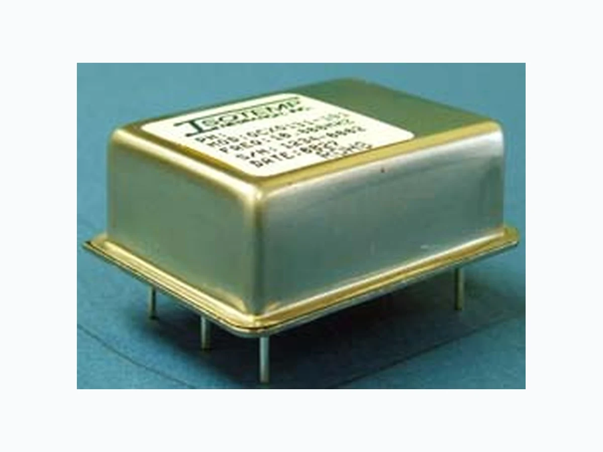
The OCXO 131 series oscillators feature small European style packages designed for applications where space is at a premium and good frequency stability is required. The oscillators can be used in phased locked loops or as stand alone references in many communications applications such as Stratum 3 switching apparatus or cellular telephone base stations. An internal voltage reference is provided to make frequency corrections via a simple potentiometer or may be used as a voltage source for a digital to analog converter. The package is a hermetically sealed through hole printed circuit board mount. A choice of quartz resonators offers a variety of performance versus cost options to fit most applications. Features: Typical 36.3 x 27.2 x 19.1 mm. SC-Cut Crystal High Stability; Low Phase Noise CMOS//Sine Wave output; Fast Warm-up
Ordering Information
(mm) Supply Voltage (V) Pulling Range (ppm) Freq. Stability (ppb) Temp. Range (ºC) Output Logic and Symmetry Oscillator Mode Pin Out Lead Free Freq. (MHz) L: 36.3 12.0 ±0.4 ± 5 0~+50 Output Symmetry Normal RoHS XX.XXXXXX 131 Series W: 27.2 5.0 ± 10 0~+70 CMOS15pF 50±10% Compliant H: 19.1 ± 20 -30~+70 Sine Wave Not RoHS ± 30 Compliant ± 50 * Not selectable by customer Please refer to "OUTLINE DRAWING" 70ºC; Sine Wave; Pin Out: Normal; RoHS Compliant; Freq. 10.000000 MHz. Freq. Stability vs. TEMP. Range ppb ±5 ±10 : ±20 Temp. (ºC) Contact e-mail: info@isotemp.com for special request INCH mm (Reference only) Outline Dra wing PIN CONNECTIONS PIN FUNCTION (See Note 1) VCO INPUT or NOT CONNECTED (See Note 1) REFERENCE VOLTAGE or NOT CONNECTED 3 + VDC 4 R.F. OUTPUT 5 0 VOLTS & CASE Note1: If the specification does not specify parameters for either PIN1 or PIN2 then that respective PIN is not internally CONNECTED.
Contact e-mail: info@isotemp.com for special request Min. Nominal Max. Note Unit Output Frequency 10.00 MHz Wave Form Sine Wave Level 6.0 8.0 10.0 dBm Load 50 Ω Harmonics -30 Spurious -60 dBc Frequency Stability Ambient ±20 Referenced to +25ºC ppb Operating Temperature -30 +70 ºC Aging * At time of shipment ±0.5 ppb After indefinite storage Daily ±0.5 After 30 days Yearly ±100
10 Years ±300
Voltage ±5 VDC ±5% change Warm-up ±20 In 5 minutes @+25ºC (Reference to 4 hours) ppb Phase Noise @ 10 MHz @ 10 Hz -120 @ 100 Hz -135 @ 1 kHz -150 @ 10 kHz -150 @ 100 kHz -150 dBc Electrical Frequency Adjustment Range 0.4 0.9 ±ppm Control 0.0 8.0 V Slope Positive Center 3.2 4.0 4.8 Control Voltage at which nominal frequency occurs at time of shipment V Input Impedance 100 KΩ Input Power Voltage 11.4 12.0 12.6 V @ turn on 3.8 Steady state @25ºC 1.5 W Reference Voltage Voltage 7.6 8.0 8.4 Optional 4.0V (Note1) 5.0V (Note2) V Load 9.0 KΩ Temperature Stability ±0.015 VDC Note 2: F or +12V CMOS Units * All aging stabilit ies are after storage of up to one year and apply after 30 days of continuous operation. ** The electronic frequenc y adjustment rage is sufficient for the life of the oscillator specification subject to change with frequency. Note 1: For all +5V input power Units The daily aging rate also applies at the time of shipment from factory.