
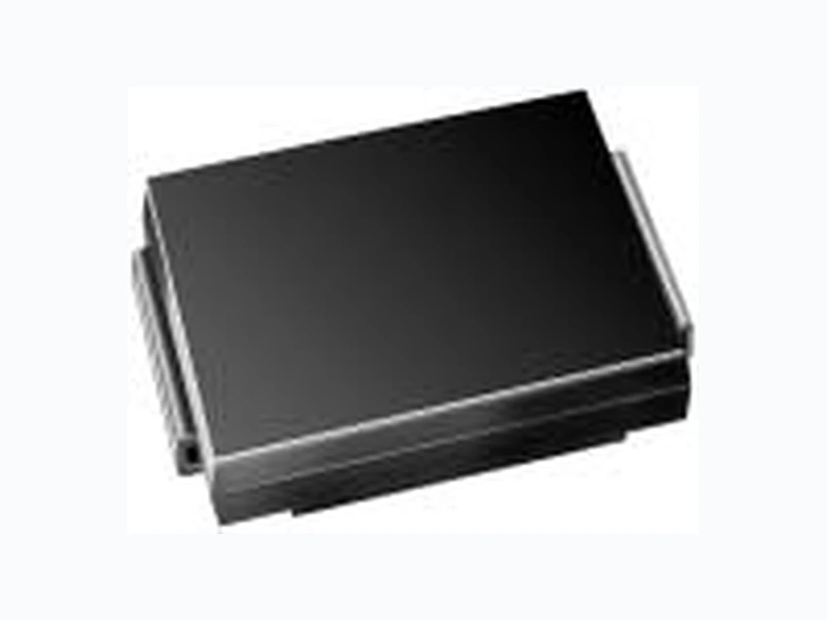
1.5SMC43CA VISHAY
Document overview
- Manufacturer or author: Provided By digicamel.com
- PDF pages: 3
Technical content
Features
- Low profile package with built-in strain relief for surface mounted applications
- Glass passivated junction
- Low incremental surge resistance
- Low inductance
- Excellent clamping capability
- 1500W peak pulse power capability with a 10/1000µs waveform, repetition rate (duty cycle): 0.01%
- Very fast response time
- Plastic package has Underwriters Laboratory Flammability Classification 94V-0 Mechanical Data Case: JEDEC DO-214AB (SMC) molded plastic over passivated junction Terminals:Solder plated, solderable per MIL-STD-750, Method 2026. High temperature soldering: 250°C/10 seconds at terminals. Polarity:For uni-directional types the band denotes the cathode, which is positive with respect to the anode under normal TVS operation. Standard Packaging:16mm tape (EIA STD RS-481) Weight:0.007 oz., 0.21 g Packaging Codes – Options (Antistatic): 51 – 1K per Bulk box, 10K/carton 57 – 850 per 7" plastic Reel (16mm tape), 8.5K/carton 9A – 3.5K per 13" plastic Reel (16mm tape), 35K/carton 0.280 (7.11) 0.260 (6.60) 0.012 (0.305) 0.006 (0.152) 0.008 (0.203) Max. 0.320 (8.13) 0.305 (7.75) 0.060 (1.52) 0.030 (0.76) 0.245 (6.22) 0.220 (5.59) 0.126 (3.20) 0.114 (2.90) 0.103 (2.62) 0.079 (2.06) Cathode Band Dimensions in inches and (millimeters) DO-214AB (SMC J-Bend) 0.185 MAX. (4.69 MAX.) 0.121 MIN. (3.07 MIN.) 0.060 MIN. (1.52 MIN.)
0.320 REF
1.5SMC Series Vishay Semiconductors formerly General Semiconductor Document Number 88303 www.vishay.com 31-Jul-03 1
Electrical Characteristics Ratings at 25°C ambient temperature unless otherwise specified. VF = 3.5V at IF = 100A (uni-directional only) Breakdown Voltage Maximum Maximum Maximum Maximum General Device Marking V (BR) at IT(1) Test Stand-off Reverse Peak Pulse Clamping Temp. Semiconductor Code (V) Current Voltage Leakage Current Voltage at Coefficient Part Number I T VWM at VWM IPPM(2) IPPM of V(BR) UNI BI MIN MAX (mA) (V) I D(4) (µA) (A) V C (V) (% / °C) Notes: (1) Pulse test: tp ≤ 50ms (2) Surge current waveform per Fig. 3 and derate per Fig. 2 (3) All terms and symbols are consistent with ANSI/IEEE CA62.35 (4) For bidirectional types with V R 10 volts and less, the ID limit is doubled 1.5SMC Series Vishay Semiconductors formerly General Semiconductor www.vishay.com Document Number 88303 2 31-Jul-03
C J — Junction Capacitance (pF) Fig. 4 – Typical Junction Capacitance Uni-Directional 100 0 7525 50 100 125 150 175 200 Peak Pulse Power (PPP ) or Current (IPP ) Derating in Percentage, % TA — Ambient Temperature (°C) 100 1,000 10,000 20,000 101 100 400 VWM — Reverse Stand-Off Voltage (V) Fig. 2 – Pulse Derating Curve PPPM — Peak Pulse Power (kW) Fig. 1 – Peak Pulse Power Rating Curve 0.1 100 0.1µs 1.0 µs1 0 µs td — Pulse Width (sec.) 100µs 1.0ms 10ms Copper Pad Areas TJ = 25°C f = 1.0MHz Vsig = 50mVp-p Measured at Zero Bias VR , Measured at Stand-Off Voltage, VWM Fig. 6 - Maximum Non-Repetitive Forward Surge Current Uni-Directional Use Only 1 10 100 100 200 Peak Forward Surge Current, Amperes Number of Cycles at 60Hz 8.3ms Single Half Sine-Wave (JEDEC Method) T J = TJ max. Uni-Directional Bi-Directional tp — Pulse Duration (sec) Transient Thermal Impedance (°C/W) Fig. 5 – Typical Transient Thermal Impedance 0.1 1.0 100 0.001 0.01 0.1 1 10 100 1000 100 150 IPPM — Peak Pulse Current, % IRSM Fig. 3 – Pulse Waveform TJ = 25°C Pulse Width (td) is defined as the point where the peak current decays to 50% of I PPM tr = 10µsec. Peak Value IPPM Half Value — IPP IPPM 2 td 10/1000µsec. Waveform as defined by R.E.A. 0 1.0 2.0 3.0 4.0 t — Time (ms) Ratings and Characteristic Curves(TA = 25°C unless otherwise noted) 1.5SMC Series Vishay Semiconductors formerly General Semiconductor Document Number 88303 www.vishay.com 31-Jul-03 3