
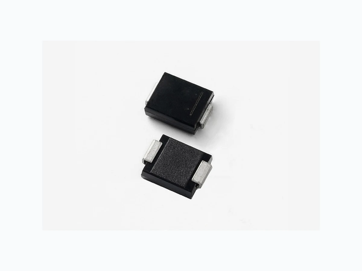
1.5SMCXXAT3G LITTELFUSE
Document overview
- Manufacturer or author: Provided By digicamel.com
- PDF pages: 5
Technical content
Features
The 1 .5SMCxxAT3G series is designed to protect voltage sensitive components from high voltage, high energy transients. They have excellent clamping capability, high surge capability, low zener impedance and fast response time. This 1 .5SMCxxAT3G series is provided in an SMC package ideally suited for small form factor requirements found in communication , automotive, process control, medical equipment and many other industrial and consumer applications.
Description
Parameter Symbol Value Unit Peak Power Dissipation (Note 1) @ TL = 25°C, Pulse Width = 1 ms PPK 1500 W DC Power Dissipation @ TL = 75°C Measured Zero Lead Length (Note 2) Derate Above 75°C Thermal Resistance from Junction−to− Lead PD R JL 4.0 54.6 18.3 W mW/°C °C/W DC Power Dissipation (Note 3) @ TA = 25°C Derate Above 25°C Thermal Resistance from Junction– to– Ambient PD RθJA 0.75 6.1 165 W mW/°C °C/W Forward Surge Current (Note 4) @ TA = 25°C IFSM 200 A Operating and Storage Temperature Range TJ, Tstg -65 to +150 °C Maximum Ratings and Thermal Characteristics 1.5SMCxxAT3G Functional Diagram Bi-directional Uni-directional Cathode Anode Pb Stresses exceeding Maximum Ratings may damage the component. Maximum Ratings are stress ratings only. Functional operation above the Recommended Operating Conditions is not implied. Extended exposure to stresses above the Recommended Operating Conditions may affect component reliability. 1 . 10 x 1000 µs, non−repetitive. 2. 1 in square copper pad, FR−4 board. 3. FR−4 board, using Littelfuse minimum recommended footprint, as shown in 403-03 case outline dimensions spec. 4. 1/2 sine wave (or equivalent square wave), PW = 8.3 ms, duty cycle = 4 pulses per minute maximum. Additional Information Samples Resources Datasheet Bi-directional Uni-directional Cathode Anode
© 2018 Littelfuse, Inc. Specifications are subject to change without notice. Revised: 02/23/18 TVS Diodes Surface Mount > 1500W > 1.5SMCxxAT3G Symbol Parameter IPP Maximum Reverse Peak Pulse Current VC Clamping Voltage @ IPP VRWM Working Peak Reverse Voltage IR Maximum Reverse Leakage Current @ VRWM VBR Breakdown Voltage @ IT IT Test Current IF Forward Current VF Forward Voltage @ IF I-V Curve Characteristics (TA = 25°C unless otherwise noted, VF = 3.5 V Max @ IF = 100 A) (Note 5) 5. 1/2 sine wave (or equivalent square wave), PW = 8.3 ms, non−repetitive duty cycle. V I
© 2018 Littelfuse, Inc. Specifications are subject to change without notice. Revised: 02/23/18 TVS Diodes Surface Mount > 1500W > 1.5SMCxxAT3G Electrical Characteristics (TA = 25°C unless otherwise noted) Component* Component Marking V RWM (Note 6) IR @ VRWM Breakdown Voltage VC @ IPP (Note 8) MV BR VBR (V) (Note 6 & 7) @ IT VC IPP Volts µA MIN NOM MAX mA Volts Amps %/ C 1 .5SMC20AT3G 20A 1 7. 1 5 19 20 21 1 27 .7 54 0.09 6. A transient suppressor is normally selected according to the maximum working peak reverse voltage (VRWM), which should be equal to or greater than the DC or continuous peak operating voltage level. 7. V BR measured at pulse test current IT at an ambient temperature of 25°C. 8. Surge current waveform per Figure 2 and derate per Figure 3 of the General Data − 1500 Watt at the beginning of this group.
© 2018 Littelfuse, Inc. Specifications are subject to change without notice. Revised: 02/23/18 TVS Diodes Surface Mount > 1500W > 1.5SMCxxAT3G Dimensions Part Marking System NOTES 1 . DIMENSIONING AND TOLERANCING PER ANSI Y14.5M, 1982. 2. CONTROLLING DIMENSION: INCH. 3. D DIMENSION SHALL BE MEASURED WITHIN DIMENSION P . 4. 403-01 THRU -02 OBSOLETE, NEW STANDARD 403-03. Soldering Footrpint Physical Specifications Case Void-free, transfer-molded, thermosetting plastic Polarity Cathode indicated by polarity band Mounting Position Any Finish All external surfaces are corrosion resistant and leads are readily solderable Leads Modified L−Bend providing more contact area to bond pads
ORDERING INFORMATION
Component Package Shipping 1SMCxxAT3G SMC (Pb−Free) 2,500 / Tape & Reel Dim Inches Millimeters Min Nom Max Min Nom Max L1 0.020 REF 0.51 REF Flow/Wave Soldering (Solder Dipping) Peak T emperature : 260OC Dipping Time : 10 seconds E bD cL1L A1 A HE D mm inches Disclaimer Notice - Information furnished is believed to be accurate and reliable. However, users should independently evaluate the suitability of and test each product selected for their own applications. Littelfuse products are not designed for, and may not be used in, all applications. Read complete Disclaimer Notice at: www.littelfuse.com/disclaimer-electronics. Specific Component Code