
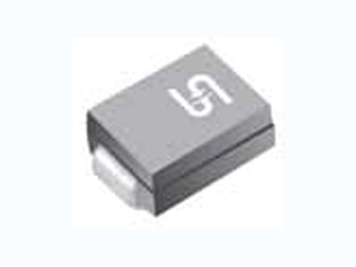
1.5SMC_1 TSC
Document overview
- Manufacturer or author: Provided By digicamel.com
- PDF pages: 4
Technical content
Features
/cuspopen For surface mounted application in order to optimize board space /cuspopen Low profile package /cuspopen Built-in strain relief /cuspopen Glass passivated junction /cuspopen Excellent clamping capability /cuspopen Fast response time: Typically less than 1.0ps from 0 volt to BV min. /cuspopen Typical I R less than 1μA above 10V /cuspopen High temperature soldering guaranteed: 260 o C / 10 seconds at terminals /cuspopen Plastic material used carries Underwriters Laboratory Flammability Classification 94V-0 /cuspopen 1500 watts peak pulse power capability with a 10 x 1000 us waveform by 0.01% duty cycle Mechanical Data /cuspopen Case: Molded plastic /cuspopen Terminals: Solder plated /cuspopen Polarity: Indicated by cathode band /cuspopen Standard packaging: 16mm tape (EIA STD RS-481) /cuspopen Weight: 0.21gram Maximum Ratings and Electrical Characteristics Rating at 25 o C ambient temperature unless otherwise specified. Type Number Symbol Value Units Peak Power Dissipation at TA=25 o C, Tp=1ms (Note 1) PPK Minimum 1500 Watts Power Dissipation on Intinite Heatsink, TA=50 o C PM(AV) 6.5 W Peak Forward Surge Current, 8.3 ms Single Half Sine-wave Superimposed on Rated Load (JEDEC method) (Note 2, 3) - Unidirectional Only IFSM 200 Amps Thermal Resistance Junction to Ambient Air (Note 4) RθJA 50 o C/W Thermal Resistance Junction to Leads RθJL 15 o C/W Operating and Storage Temperature Range TJ, TSTG -55 to + 150 o C Notes: 1. Non-repetitive Current Pulse Per Fig. 3 and Derated above T A=25 o C Per Fig. 2. 2. Mounted on 8.0mm (.013mm Thick) Copper Pads to Each Terminal. 3. 8.3ms Single Half Sine-wave or Equivalent Square Wave, Duty Cycle=4 Pulses Per Minute Maximum. 4. Mounted on 5.0mm (.013mm thick) land areas. Devices for Bipolar Applications 2. Electrical Characteristics Apply in Both Directions.
- 547 - RATINGS AND CHARACTERISTIC CURVES (1.5SMC SERIES) FIG.1- PEAK PULSE POWER RATING CURVE P , PEAK PULSE POWER, KW PPM tp, PULSE WIDTH, sec. NON-REPETITIVE PULSE WAVEFORM SHOWN in FIG.3 T = 25 C A O 0.1 s 1s 10 s 100 s 1.0ms 10ms 0.1 100 FIG.3- PULSE WAVEFORMCLAMPING POWER PEAK PULSE CURRENT t, TIME, ms td tr = 10 sec PULSE WIDTH (td) is DEFINED as the POINT WHERE the PEAK CURRENT DECAYS to 50% of I PPMPeak Value I PPM Half Value - IPPM 10/1000 sec. WAVEFORM as DEFINED by R.E.A. 0 1.0 2.0 3.0 4.0 100 150 FIG.2- PULSE DERATING CURVE PEAK PULSE POWER (P ) or CURRENT (I ) PP PPM TA, AMBIENT TEMPERATURE. ( C) O DERATING IN PERCENT AGE. % 0 25 50 75 100 125 150 175 200 100 150 200 FIG.5- TYPICAL JUNCTION CAPACITANCE UNIDIRECTIONAL CJ, JUNCTION CAP ACITANCE. (pF) V( ), BREAKDOWN VOLTAGE. VOLTSBR UNIDIRECTIONAL BIDIRECTIONA V= 0R Tj = 25 C f=1.0MHz Vsig=50mVp-p O V -RATED STAND-OFF VOLTAGE R 1 10 100 200 100 1000 10000 FIG.4- MAXIMUM NON-REPETITIVE FORWARD SURGE CURRENT UNIDIRECTIONAL ONLY NUMBER OF CYCLES AT 60Hz I , PEAK FOR WARD SURGE CURRENT FSM AMPERES 8.3ms Single Half Sine Wave JEDEC Method Tj=Tj max. 1 10 100 100 200 Version: A06
Dimensions in inches and (millimeters) - 548 - ELECTRICAL CHARACTERISTICS (TA=25 OC unless otherwise noted) Test Stand-Off Maximum Maximum Maximum Maximum GENERAL Device Current Voltage Reverse Leakag e Peak Surge Clamping Temperature PART Marking @IT VWM at Vwm Current I PPM Voltage at IPPM Coefficient NUMBER Code Min Max (mA) (Volts) I D (uA) (Note 2)(Amps) V C(Volts) of V BR(% / OC) Breakdown Voltage VBR (Volts) (Note 1)
- 549 - ELECTRICAL CHARACTERISTICS (TA=25OC unless otherwise noted) Breakdown Voltage Stand-Off Maximum Max imum Maximum Maximum GENERAL Device VBR Test Current Voltage Reverse Leaka ge Peak Surge Clamping Temperature PART Marking (Volts) (Note 1) @IT(mA) V WM at Vwm Current I PPM Voltage at IPPM Coefficient NUMBER Code Min Max (Volts) I D (uA) (Note 2)(Amps) V C(Volts) of V BR(% / OC) Notes: 1. VBR measured after IT applied for 300us, IT =square wave pulse or equivalent. 2. Surge current waveform per Figure 3 and derate per Figure 2. 3. For bipolar types having VWM of 10 volts and under, the ID limit is doubled. 5. All terms and symbols are consistent with ANSI/IEEE C62.35.