
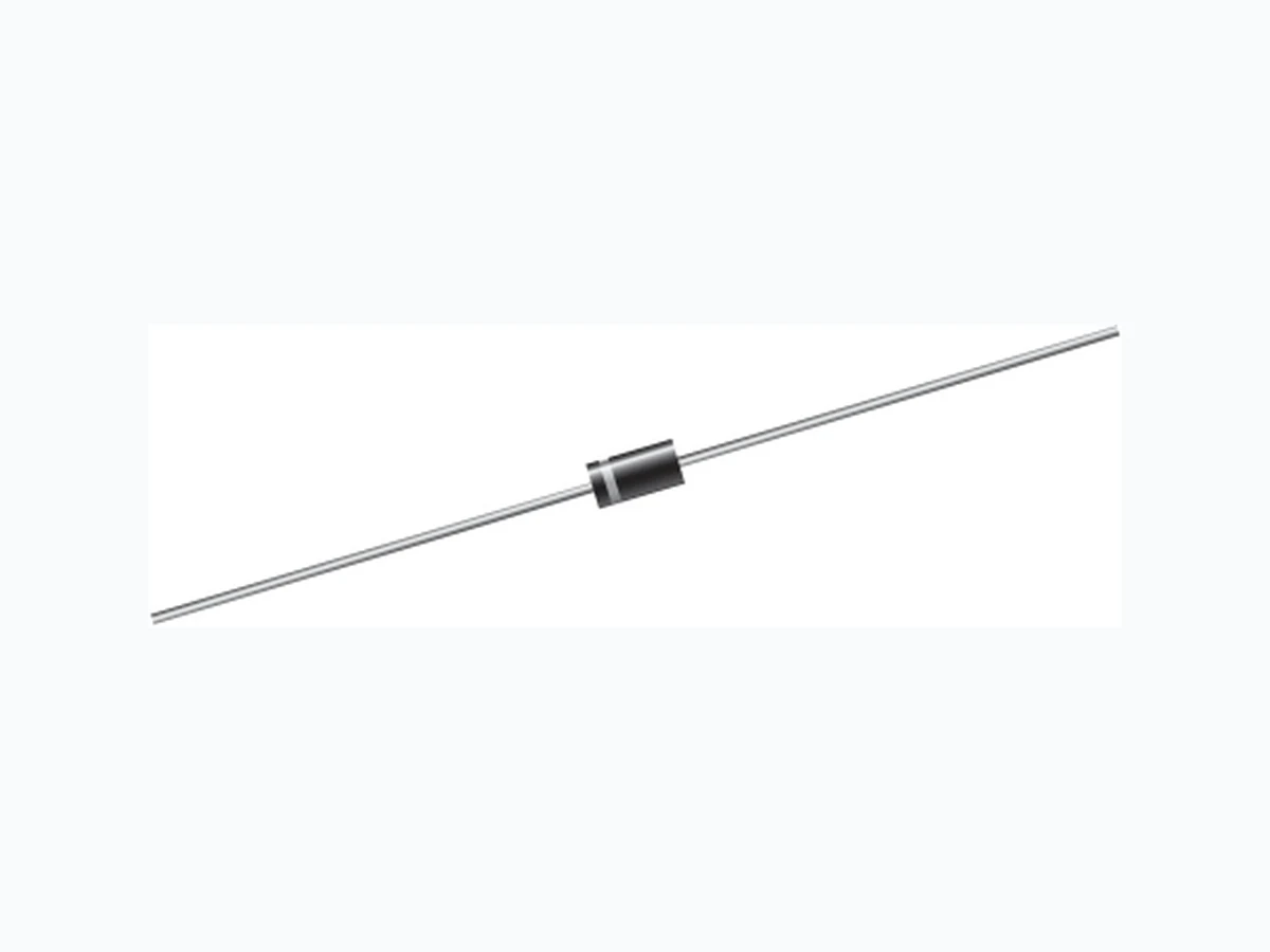
1.5KE-G COMCHIP
Document overview
- Manufacturer or author: Provided By digicamel.com
- PDF pages: 5
Technical content
Features
-Plastic package has underwriters laboratory flammability classification 94V-0 -1500W, surge capability at 1mS. -Excellent clamping capability. -Low Zener impedance. -Fast response time: typically less than 1.0pS from 0 volt to BV min. -Typical IR less than 1μA above 10V. -High temperature soldering guaranteed: O 260 C/10S/0.375"(9.5mm) lead length/5lbs.,(2.3KG) tension Mechanical Data -Case: Molded plastic DO-201AE -Terminals: Axial leads, solderable per MIL-STD- 202, Method 208 -Polarity: Color band denotes cathode except bipolar -Weight: 1.2 gram Dimensions in inches and (millimeter) DO-201AE Peak forward surge current, 8.3mS single half sine-wave superimposed on rated load (JEDEC method) (Note 3) Operating junction and storage temperature range PPK 5.0 Maximum 1500 -55 to +175 W W A O C O Steady state power dissipation at TL=75 C Lead length 0.375" (9.5mm) (Note 2) NTOES: O (1) Non-repetitive current pulse, per fig.3 and derated above TA=25 C per fig. 2.2 2 (2) Mounted on copper land area of 0.79in (20mm ). (3) 8.3mS single half-sine wave, duty cycle=4 pulses per minute maximum. (4) For bidirectional use C suffix for 10% tolerance, CA suffix for 5% tolerance. PD IFSM TJ, TSTG 1.0(25.4) MIN. 0.375(9.5) 0.335(8.5) 0.220(5.6) 0.197(5.0) 0.042(1.07) 0.037(0.94) 1.0(25.4) MIN.
RATING AND CHARACTERISTIC (1.5KE-G Series) 1500W Transient Voltage Suppressor1500W Transient Voltage Suppressor Page 2QW-BTV07 REV:A SMD Diodes Specialist M IN . M A X. P art N o. M axim um C lam ping V oltage V R W M (V ) M axim um T em perature C oefficient of V B R (% C ) V B R (V ) @ IT(m A ) B reakdow n V oltage W orking P eak R everse V oltage V R W M (V ) M axim um R everse Leakage at V R W M IR (μ A ) M axim um R everse C urrent IR S M (A )
1500W Transient Voltage Suppressor1500W Transient Voltage Suppressor Page 3QW-BTV07 REV:A SMD Diodes Specialist RATING AND CHARACTERISTIC (1.5KE-G Series) NOTES: 1. VBR measured after IT applied for 300μS, IT=square wave pulse or equivalent. 2. Surge current wave form per fig.3 and derated per fig.2. 3. VF=3.5V at IF=50A (P6KE6.8-G thru P6KE91A-G VF=5.0V at IF=50A (p6KE100-G thru P6KE400A-G on ½ square or equivalent sine wave. PW=8.3mS, duty cycle=4 pulses per minute max.. 4. For bipolar types having VRWM of 10 Volts and under, the IR limit is doubled. MIN. MAX. Part No. Maximum Clamping Voltage VRW M (V) Maximum Temperature Coefficient of VBR (%C) VBR (V) @IT(mA) Breakdown Voltage W orking Peak Reverse Voltage VRW M(V) Maximum Reverse Leakage at VRW M IR(μA) Maximum Reverse Current IRSM (A)
RATING AND CHARACTERISTIC CURVES (1.5KE-G Series) 1500W Transient Voltage Suppressor1500W Transient Voltage Suppressor Page 4QW-BTV07 REV:A SMD Diodes Specialist Fig.2 Pulse Derating Curve Peak Pulse Power (PPP) or Current(IPP) Derating in Percentge (%) O TA, Ambient Temperature ( C) Fig.1 Peak Pulse Power Rating Curve 0.1 PPPM,Peak Pulse Power (kW) td, Pulse Width (sec) 0.1μS 1.0μS 10μS 100μS 1.0mS 10mS 1.0 100 100 50 100 200 Fig.3 Pulse Wave Form IPPK, Peak Pulse Current (%) t, Time (mS) 0 1 2 3 4 100 150 Fig.4 Typical Junction Capacitance Unidirectional CJ, Junction Capacitance (pF) VBR, Breakdown Voltage (V) 500 100 1000 10000 Fig.5 Steady State Power Derating Curve PM(AV), Steady State Power Dissipation (W) O TL, Lead Temperature ( C) 0 50 75 150 200 5.00 1.25 150 tr=10μS Peak value, IPPM Half value, IPP/2 10/1000μS waveform as deined by R.E.A Pulse width (td) is defined as the point where the peak current decays to 50% of IPP td 100 25 100 125 175 2.50 3.75 Fig.6 Maximum Non-repetitive Forward Surge Current Unidirectional IFSM, Peak Forward Surge Current (A) Number of Cycles at 60Hz 8.3mS single half sine-wave (JEDEC method) 10 100 100 200 60Hz Resistive or inductive load 1.6" 1.6" 0.040" (40"X40"X 1mm) Copper heat sinks L=0.375"(9.5mm) Lead lengths Non-repetitive pulse waveform shown in fig.3 O TA=25 C f=1MHz Vsig=50mVp-pO Tj=25 C VR=Rated stand-off voltage VR=0 Unidirectional Bidirectional
RATING AND CHARACTERISTIC CURVES (1.5KE-G Series) 1500W Transient Voltage Suppressor1500W Transient Voltage Suppressor Page 5QW-BTV07 REV:A SMD Diodes Specialist Fig.7 Incremental Clamping Voltage Curve Unidirectional ΔVC, Incremental Clamping Voltage IPP, Peak Pulse Current (A) 0.1 0.5 1 10 50 100 Waveform: 10X1000 impulse ΔVC=VC-VBR 1.5KE200 1.5KE130 1.5KE100 1.5KE75 1.5KE39 1.5KE33 1.5KE6.8 1.5KE9.1 1.5KE18 1.5KE12 Waveform: 10X1000 impulse ΔVC=VC-VBR 1.5KE200 1.5KE130 1.5KE75 1.5KE39 1.5KE33 1.5KE6.8 1.5KE9.1 Fig.8 Incremental Clamping Voltage Curve Unidirectional 0.1 ΔVC, Incremental Clamping Voltage IPP, Peak Pulse Current (A) 0.5 1 10 50 100 Waveform: 10X1000 impulse ΔVC=VC-VBR 1.5KE200C 1.5KE75C 1.5KE39C 1.5KE30C 1.5KE7.5C 1.5KE11C 1.5KE15C Fig.9 Incremental Clamping Voltage Curve Bidirectional 0.1 ΔVC, Incremental Clamping Voltage IPP, Peak Pulse Current (A) 0.5 1 10 50 100 Fig.10 Incremental Clamping Voltage Curve Bidirectional 0.1 ΔVC, Incremental Clamping Voltage IPP, Peak Pulse Current (A) 0.5 1 10 50 100 Waveform: 10X1000 impulse ΔVC=VC-VBR 1.5KE200C 1.5KE75C 1.5KE39C 1.5KE30C 1.5KE7.5C 1.5KE11C 1.5KE15C Fig.11 Instantaneous Forward Voltage Characteristics Curve 0.1 Forward Current Instantaneous Forward Current (A) Pulse width=300μS 1% duty cycleO TJ=25 C 100 Fig.12 Breakdown Voltage Temperature Coefficient Curve O Temperature Coefficient (mV/ C) VBR, Breakdown Voltage (V) 100 1000 10 100 500 Unidirectional Bidirectional