
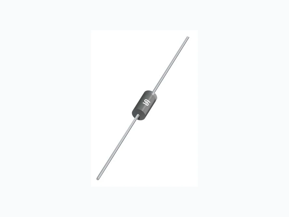
1.5KE_15 TSC
Document overview
- Manufacturer or author: Provided By digicamel.com
- PDF pages: 6
Technical content
- Excellent clamping capability - Low dynamic impedance - 1500W surge capability at 10 / 1000 μs waveform - Typical I R less than 1μA above 10V - Halogen-free according to IEC 61249-2-21 definition Molding compound, UL flammability classification rating 94V-0 Part No. with suffix "H" means AEC-Q101 qualified Packing code with suffix "G" means green compound (halogen-free) Terminal: Pure tin plated leads, solderable per JESD22-B102 Meet JESD 201 class 2 whisker test SYMBOL UNIT P PK Watts TJ °C TSTG °C Note 3: VF=3.5V for Devices of VBR≦200V and VF=5.0V Max. for Devices VBR>200V Devices for Bipolar Applications 1. For Bidirectional Use C or CA Suffix for Types 1.5KE6.8 - Types 1.5KE440 2. Electrical Characterstics Apply in Both Directions PART NO. Note 1: "xxxx" defines voltage from 6.8V (1.5KE6.8) to 440V (1.5KE440) PART NO. Document Number: DS_D1409026 Version: M15 AEC-Q101 qualified Green compound1.5KE100AHR0G 1.5KE100A H R0 G DO-201 500 / Bulk packing EXAMPLE PREFERRED PART NO. PART NO. SUFFIX PACKING CODE PACKING CODE SUFFIX
DESCRIPTION
1.5KExxxx (Note 1) H G DO-201 500 / Ammo box R0 DO-201 1,250 / 13" Paper reel
ORDERING INFORMATION
PART NO. SUFFIX PACKING CODE PACKING CODE SUFFIX PACKAGE PACKING Storage temperature range - 55 to +175 Note 1: Non-repetitive Current Pulse Per Fig. 3 and Derated above TA=25°C Per Fig. 2 Note 2: Mounted on Copper Pad Area of 0.6" x 0.6" (16mm x 16mm) Maximum Instantaneous Forward Voltage at 50 A for Unidirectional Only (Note 3) VF 3.5 / 5.0 Volts Operating junction temperature range MAXIMUM RATINGS AND ELECTRICAL CHARACTERISTICS (TA=25°C unless otherwise noted) - 55 to +175 Peak power dissipation at TA=25°C, Tp=1ms (Note 1) 1500 Peak forward surge current, 8.3 ms single half sine-wave superimposed on rated load IFSM 200 - UL recognized file # E-326243 A Steady state power dissipation at TL=75°C lead lengths .375", 9.5mm (Note 2) PD Watts5 DO-201 MECHANICAL DATA Case: DO-201 Weight: 0.94g (approximately) PARAMETER VALUE 1.5KE SERIES Taiwan Semiconductor 1500W, 6.8V - 440V Transient Voltage Suppressor
FEATURES
- Fast response time: Typically less than 1.0ps from 0 volt to VBR for unidirectional and 5.0ns for bidirectional - Compliant to RoHS Directive 2011/65/EU and in accordance to WEEE 2002/96/EC
Document Number: DS_D1409026 Version: M15 RATINGS AND CHARACTERISTICS CURVES (TA=25°C unless otherwise noted) 1.5KE SERIES Taiwan Semiconductor 100 125 0 25 50 75 100 125 150 175 200 PEAK PULSE POWER(PPP) OR CURRENT (IPP) A DERATING IN PERCENTAGE (%) TA, AMBIENT TEMPERATURE (oC) FIG.2 PULSE DERATING CURVE With heat sink Without heat sink 100 120 140 160 180 200 1 10 100 IFSM, PEAK FORWARD SURGE CURRENT (A) NUMBER OF CYCLES AT 60 Hz FIG. 4 MAXIMUM NON-REPETITIVE FORWARD SURGE CURRENT UNIDIRECTIONAL ONLY 8.3ms Single Half Sine Wave 100 120 140 00 . 511 . 522 . 533 . 54 PEAK PULSE CURRENT (%) t, TIME ms FIG. 3 CLAMPING POWER PULSE WAVEFORM td Peak Value IPPM tr=10μs Half Value-IPPM/2 10/1000μs, WAVEFORM as DEFINED by R.E.A. PULSE WIDTH(td) is DEFINED as the POINT WHERE the PEAK CURRENT DECAYS to 50% OF IPPM 100 1000 10000 1 10 100 CJ, JUNCTION CAPACITANCE (pF) A V(BR), BREAKDOWN VOLTAGE (V) FIG. 5 TYPICAL JUNCTION CAPACITANCE f=1.0MHz Vsig=50mVp-p VR=0 VR-RATED STAND-OFF VOLTAGE UNIDIRECTIONAL BIDIRECTIONA 0.1 100 0.1 1 10 100 1000 10000 PPPM, PEAK PULSE POWER, kW tp, PULSE WIDTH, (μS) FIG. 1 PEAK PULSE POWER RATING CURVE NON-REPETITIVE PULSE WAVEFORM SHOWN in FIG.3
Test Stand-Off Maximum Maximum Maximum Maximum Current Voltage Reverse Leakage Peak Pulse Clamping Voltag e Temperature IT VWM @ VWM Current IPPM @ IPPM Coefficient VM i n M a x ( m A ) ( V ) ID (μA) (A) (Note 2) Vc(V) of VBR(%/°C) Document Number: DS_D1409026 Version: M15 1.5KE SERIES Taiwan Semiconductor JEDEC TYPE NUMBER GENERAL PART NUMBER Breakdown Voltage VBR (V) (Note 1) Nominal Voltage
Test Stand-Off Maximum Maximum Maximum Maximum Current Voltage Reverse Leakage Peak Pulse Clamping Voltag e Temperature IT VWM @ VWM Current IPPM @ IPPM Coefficient VM i n M a x ( m A ) ( V ) ID (μA) (A) (Note 2) Vc(V) of VBR(%/oC) 1N6297A 1.5KE120A 120 114 126 1.0 102 1 9.5 165 0.107 1N6298 1.5KE130 130 117 143 1.0 105 1 8.4 187 0.107 1N6298A 1.5KE130A 130 124 137 1.0 111 1 8.7 179 0.107 1N6299 1.5KE150 150 135 165 1.0 121 1 7.3 215 0.108 1N6299A 1.5KE150A 150 143 158 1.0 128 1 7.6 207 0.108 1N6300 1.5KE160 160 144 176 1.0 130 1 6.8 230 0.108 1N6300A 1.5KE160A 160 152 168 1.0 136 1 7.1 219 0.108 1N6301 1.5KE170 170 153 187 1.0 138 1 6.4 244 0.108 1N6301A 1.5KE170A 170 162 179 1.0 145 1 6.7 234 0.108 1N6302 1.5KE180 180 162 198 1.0 146 1 6.1 258 0.108 1N6302A 1.5KE180A 180 171 189 1.0 154 1 6.4 246 0.108 1N6303 1.5KE200 200 180 220 1.0 162 1 5.4 287 0.108 1N6303A 1.5KE200A 200 190 210 1.0 171 1 5.7 274 0.108 1.5KE220 220 198 242 1.0 175 1 4.5 344 0.110 1.5KE220A 220 209 231 1.0 185 1 4.8 328 0.110 1.5KE250 250 225 275 1.0 202 1 4.3 360 0.110 1.5KE250A 250 237 263 1.0 214 1 4.5 344 0.110 1.5KE300 300 270 330 1.0 243 1 3.6 430 0.110 1.5KE350 350 315 385 1.0 284 1 3.1 504 0.110 1.5KE350A 350 333 368 1.0 300 1 3.2 482 0.110 1.5KE400 400 360 440 1.0 324 1 2.7 574 0.110 1.5KE400A 400 380 420 1.0 342 1 2.8 548 0.110 1.5KE440 440 396 484 1.0 356 1 2.4 631 0.110 1.5KE440A 440 418 462 1.0 376 1 2.5 602 0.110 Notes: 1. V BR measure after IT applied for 300 μs, IT=square wave pulse or equivalent. 2. Surge current waveform per Figure. 3 and derate per Figure. 2. 3. For bipolar types having VWM of 10 volts and under, the ID limit is doubled. 4. All terms and symbols are consistent with ANSI/IEEE C62.35. Document Number: DS_D1409026 Version: M15 1.5KE SERIES Taiwan Semiconductor JEDEC TYPE NUMBER GENERAL PART NUMBER Breakdown Voltage VBR (V) (Note 1) Nominal Voltage
A 5.00 5.60 0.197 0.220 B 0.96 1.06 0.038 0.042 C 25.40 - 1.000 - D 8.50 9.50 0.335 0.375 E 25.40 - 1.000 - P/N = Specific Device Code G = Green Compound YWW = Date Code F = Factory Code Document Number: DS_D1409026 Version: M15 MARKING DIAGRAM 1.5KE SERIES Taiwan Semiconductor DIM. Unit (mm) Unit (inch) PACKAGE OUTLINE DIMENSIONS DO-201
assumes no responsibility or liability for any errors or inaccuracies. Information contained herein is intended to provide a product description only. No license, express or implied, to any intellectual property rights is granted by this document. Except as provided in TSC's terms and conditions of sale for such products, TSC assumes no liability whatsoever, and disclaims any express or implied warranty, relating to sale and/or use of TSC products including liability or warranties relating to fitness for a particular purpose, merchantability, or infringement of any patent, copyright, or other intellectual property right. The products shown herein are not designed for use in medical, life-saving, or life-sustaining applications. Customers using or selling these products for use in such applications do so at their own risk and agree to fully indemnify TSC for any damages resulting from such improper use or sale. Document Number: DS_D1409026 Version: M15 1.5KE SERIES Taiwan Semiconductor Notice Specifications of the products displayed herein are subject to change without notice. TSC or anyone on its behalf,