

 Download PDF
DATASHEET SEARCH SITE
Document overview
- PDF pages: 4
Technical content
Page 1
MLOTM TECHNOLOGY
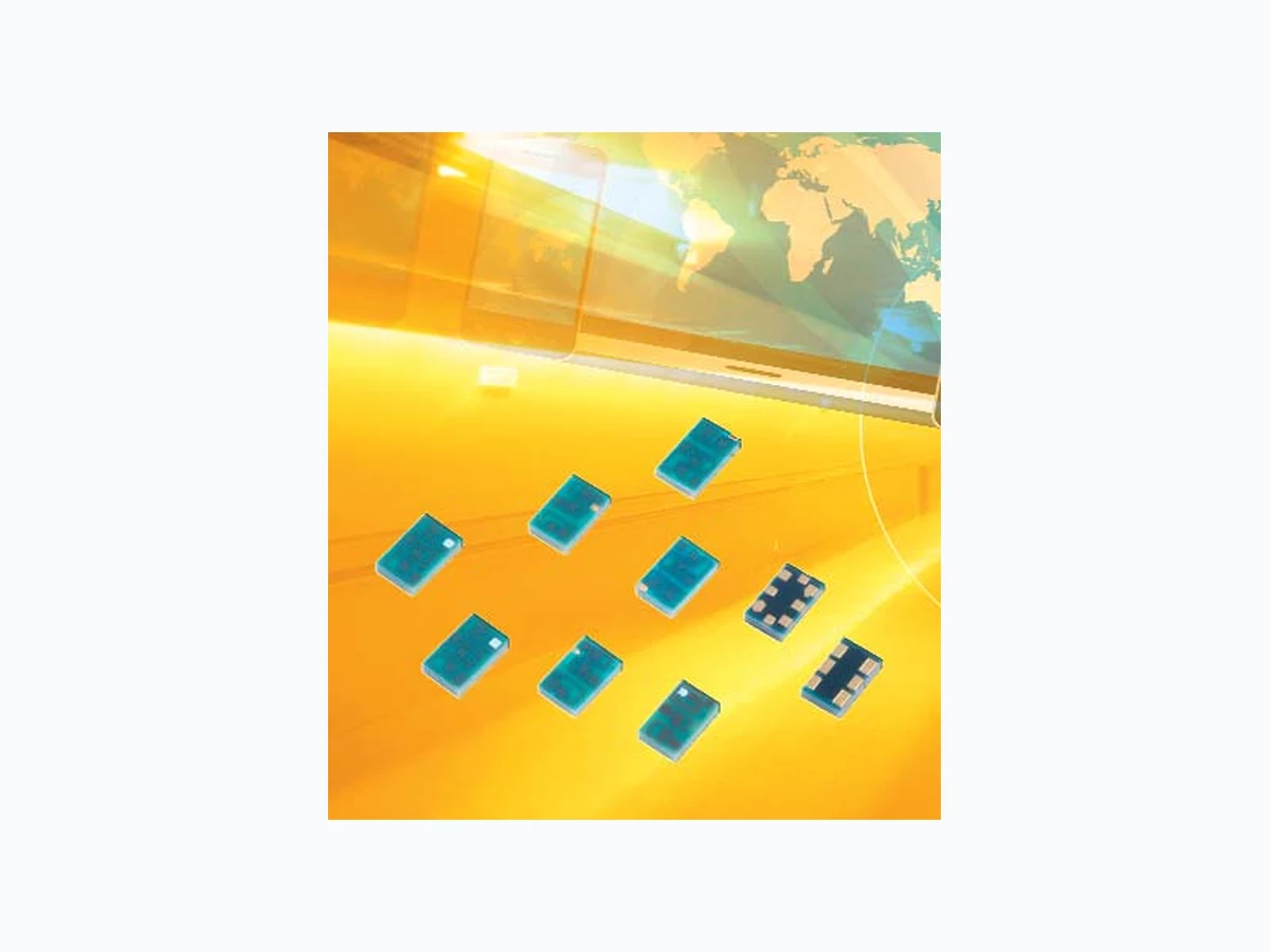
The 0806 diplexer is a best in class low profile multilayer organic passive device that is based on AVX’s patented multilayer organic high density interconnect technology. The MLOTM diplexer uses high dielectric constant and low loss materials to realize high Q passive printed passive elements such as inductors and capacitors in a multilayer stack up. The MLOTM diplexers can support multiple wireless standards such as WCDMA, CDMA, WLAN, and GSM and are less than 0.6mm in thickness. These components are ideally suited for band switching for dual band systems. All diplexers are expansion matched to FR4 thereby resulting in improved reliability over standard
Si and ceramic devices.
APPLICATIONS
Multiband applications including WCDMA, WLAN, WiMax, GPS, and cellular bands
LAND GRID ARRAY
ADVANTAGES
- Low Insertion Loss
- Excellent Solderability
- Low Parasitics
- Low Profile
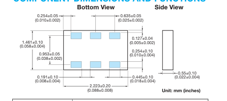
COMPONENT DIMENSIONS AND FUNCTIONS
HOW TO ORDER
DP 06 B
1945
7 TR
Type Size Design Frequency
Finish Packaging
(MHz) 7 = Au Tape & Reel T = NiSn
QUALITY INSPECTION
Finished parts are 100% tested for electrical parameters and visual characteristics.
| Terminal No. | Terminal Name |
|---|---|
| 1 | Low Frequency Port |
| 2 | GND |
| 3 | High Frequency Port |
| 4 | GND |
| 5 | Common Port |
| 6 | GND |
OPERATING TEMPERATURE
-40ºC to +85ºC
TERMINATION
Finishes available in Ni/Sn, Immersion Sn, Immersion Au and OSP coatings which are compatible with automatic soldering technologies which include reflow, wave
0806 CDMA DIPLEXER SPECIFICATIONS
soldering, vapor phase and manual.
PART NUMBER: DP06B1945TTR
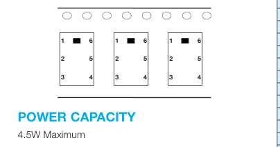
ORIENTATION IN TAPE
| Specification | AVX -MLOTM mm (inches) |
| Size | 2.2 x 1.5 (0.083 x 0.060) |
| Height | 0.55 (0.021) |
| Volume (mm^3) | 1.75 |
| Frequency Range (F1) (MHz) | 730 ± 230 MHz |
| Frequency Range (F2) (MHz) | 2200 ± 500 MHz |
| Insertion Loss (F1, at Fc @ 25oC) | -0.4 |
| Insertion Loss (F1 at Fc) (-40 to 85ºC) | - 0.55 |
| Insertion Loss (F2, at Fc @ 25ºC) | -0.5 |
| Insertion Loss (F1 at Fc ) (-40 to 85ºC) | -0.65 |
| Attenuation (F1) at (F2) (dB min) | -22 |
| Attenuation (F2) at (F1) (dB min) | -22 |
| VSWR (Input @ F1) | 1.2 |
| VSWR (Input @ F2) | 1.6 |
| VSWR (Lowband @ F1) | 1.3 |
| VSWR (Highband @ F2) | 1.7 |
Page 2
S PARAMETER MEASUREMENTS
INSERTION LOSS
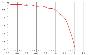
Frequency (GHz)
Low Band Insertion Loss
| Frequency (GHz) | Insertion Loss (dB) |
| 0.500 | 0.121 |
| 0.698 | 0.199 |
| 0.960 | 0.400 |
ATTENUATION
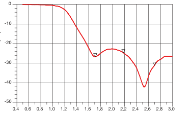
Frequency (GHz)
Low Band Attenaution
| Frequency (GHz) | Attenuation (dB) |
| 1.710 | 26.726 |
| 2.180 | 24.681 |
| 2.700 | 31.074 |
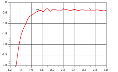
Frequency (GHz)
High Band Insertion Loss
| quency (GHz) | Insertion Loss (dB) |
| 1.710 | 0.430 |
| 2.180 | 0.352 |
| 2.700 | 0.360 |
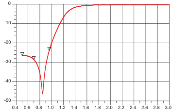
Frequency (GHz)
High Band Attenaution
| quency (GHz) | Attenuation (dB) |
| 0.500 | 26.671 |
| 0.698 | 28.611 |
| 0.960 | 23.988 |
Page 3
RETURN LOSS
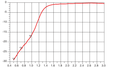
Frequency (GHz)
Low Band Return Loss
| quency (GHz) | Insertion Loss (dB) |
| 0.500 | 29.191 |
| 0.698 | 23.723 |
| 0.960 | 17.655 |
COMMON RETURN LOSS
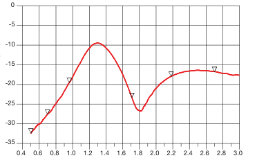
Frequency (GHz)
Common Port Return Loss
| quency (GHz) | Attenuation (dB) |
| 0.500 | 32.382 |
| 0.698 | 27.566 |
| 0.960 | 19.543 |
| 1.710 | 23.343 |
| 2.180 | 17.958 |
| 2.700 | 16.744 |
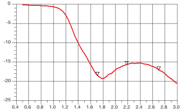
Frequency (GHz)
High Band Return Loss
Frequency (GHz)
Insertion Loss (dB)
1.710
18.487
2.180
15.685
2.700
17.037
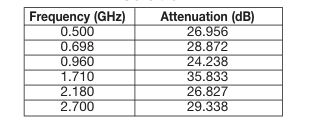
ISOLATION
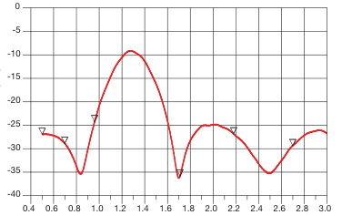
Frequency (GHz)
Isolation
Page 4
AUTOMATED SMT ASSEMBLY
The following section describes the guidelines for automated SMT assembly of MLOTM RF devices which are typically Land Grid Array (LGA) packages or side termination SMT pacages. Control of solder and solder paste volume is critical for surface mount assembly of MLOTM RF devices onto the PCB.
SMT REFLOW PROFILE
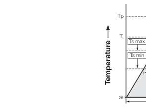
Common IR or convection reflow SMT processes shall be used for the assembly. Standard SMT reflow profiles, for eutectic and Pb free solders, can be used to surface mount the MLOTM devices onto the PCB. In all cases, a temperature gradient of 3°C/sec, or less, should be maintained to prevent warpage of the package and to ensure that all joints reflow properly. Additional soak time and slower preheating time
Stencil thickness and aperture openings should be adjusted according to the optimal solder volume. The following are general recommendations for SMT mounting of MLOTM devices onto the PCB.
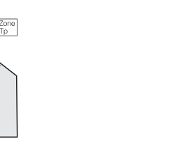
may be required to improve the out-gassing of solder paste. In addition, the reflow profile depends on the PCB density and the type of solder paste used. Standard no-clean solder paste is generally recommended. If another type of flux is used, complete removal of flux residual may be necessary. Example of a typical lead free reflow profile is shown below.
| tp Critical Zone T to Tp Ramp-up L Ts max t L Ts min ts Ramp-down Preheat | |
|---|---|
| t 25ºC to Peak | |
Time
Figure A. Typical Lead Free Profile and Parameters
| Profile Parameter | Pb free, Convection, IR/Convection |
|---|---|
| Ramp-up rate (Tsmax to Tp | 3ºC/second max. |
| Preheat temperature (Ts min to Ts max) | 150ºC to 200ºC |
| Preheat time (ts) | 60 – 180 seconds |
| Time above T , 217ºC (t ) L L | 60 – 120 seconds |
| Peak temperature (Tp) | 260°C |
| Time within 5ºC of peak temperature (tp) | 10 – 20 seconds |
| Ramp-down rate | 4ºC/second max. |
| Time 25ºC to peak temperature | 6 minutes max. |