
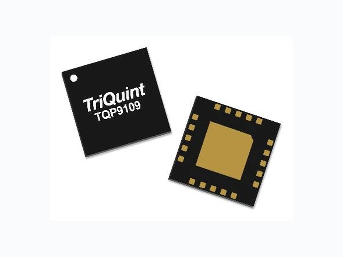
TQP9109 QORVO
Document overview
- Manufacturer or author: Provided By digicamel.com
- PDF pages: 11
Technical content
1/2 W 2-stage Linear Amplifier Datasheet, January 30, 2018 | Subject to change without notice - 1 of 11 - www.qorvo.com 4x4 mm Leadless SMT Package Key Features
- 1.7 – 2.7 GHz Frequency Range
- 30.5 dB gain
- +27.5 dBm P1dB
- +46 dBm Output IP3
- Input Internally Matched
- Integrated interstage matching
- Power down functionality for second stage amp
- Bias Adjustable Product Description The TQP9109 is a high efficiency two -stage driver amplifier in a low -cost surface -mount package. The amplifier is able to achieve high performance with +46 dBm OIP3 and +27.5 dBm P1dB while only consuming 245 mA current. The linear amplifier i ntegrates two high performance amplifier stages onto a module to allow for a compact system design. The input is internally matched and the amplifier only requires minimal external components for operation. The integrated interstage match minimizes perfor mance variation that would otherwise be attributed to external matching component value and placement tolerances. The output stage amplifier is bias adjustable allowing the amplifier’s power consumption to be reduced for occasions when the high power per formance is not required. The output stage can also be turned off when not being used for power savings. The output match is tunable externally to allow the amplifier to be optimized for high power or high linearity applications. Up to 46 dBm OIP3 can be achieved when optimized for linearity. The TQP9109 is available in a RoHS-compliant 20-pin 4x4mm surface mount package.
Applications
- Wireless Infrastructure
- Repeaters, Boosters, DAS
- High Power Amplifiers
- Pico and Macro Basestations Functional Block Diagram Top View
Ordering Information
Part No. Description TQP9109 2,500 pieces on a 13” reel (standard) TQP9109-PCB2140 1.8 − 2.2 GHz Evaluation Board TQP9109-PCB2600 2.3 − 2.7 GHz Evaluation Board Exposed Backside Pad GND Pin 1 Reference Mark Package Topside NC RFin RFin RFin NC NC RFout RFout RFout NC Vcc1 NC VCC2 NC NC NC NC Iref NC NC
1/2 W 2-stage Linear Amplifier Datasheet, January 30, 2018 | Subject to change without notice - 2 of 11 - www.qorvo.com Recommended Operating Conditions Parameter Min Typ Max Units Supply Voltage (VCC1, VCC2) +4.75 +5 +5.25 V TCASE −40 +105 °C Tj for >106 hours MTTF +170 °C Electrical specifications are measured at specified test conditions. Specifications are not guaranteed over all recommended operating conditions. Absolute Maximum Ratings Parameter Rating Storage Temperature −50 to +150 °C RF Input Power, CW, 50Ω, T=+25 °C +8 dBm Supply Voltage (VCC1, VCC2) +6 V Exceeding any one or a combination of the Absolute Maximum Rating conditions may cause permanent damage to the device. Extended application of Absolute Maximum Rating conditions to the device may reduce device reliability. Electrical Specifications Test conditions unless otherwise noted: Supply Voltage =+5 V, ICQ = 237 mA, IREF = 8 mA, TCASE = +25 °C Parameter Conditions Min Typ Max Units Frequency Range 1700 2700 MHz Test Frequency 2140 MHz Gain 27.5 29.9 32.5 dB Input Return Loss 11 dB Output Return Loss 14 dB Output P1dB +25.0 +27.9 dBm Output IP3 Pout= +11 dBm/tone, Δf=1 MHz +41.0 +45.8 dBm Noise Figure 3.5 dB Total Current ICQ1 + ICQ2 + IREF 210 239 280 mA Current, ICQ1 89 mA Current, ICQ2 150 mA Current, IREF 8 mA Thermal Resistance, θjc Module (junction to case) 36.2 °C/W
1/2 W 2-stage Linear Amplifier Datasheet, January 30, 2018 | Subject to change without notice - 3 of 11 - www.qorvo.com Evaluation Board – TQP9109-PCB2140 Bill of Material – TQP9109-PCB2140 Ref Des Value Description Manuf. Part Number U1 AMP, 4x4mm SMT Module, 2-stage, Linear Qorvo TQP9109 C1, C5, C13, C15 0.1 uF CAP, 0603,10%, 50V, X7R various C2 1000 pF CAP, 0603, 5%, 50V, NPO various C3 100 pF CAP, 0603, 5%, 50V, NPO various Z1 0.5 pF CAP, 0402, +/-0.1pF, 50V, NPO/COG AVX 04025A0R5BAT2A C9 10 Ω RES, 0603, 1%, 1/16W, Chip various Z4 2.2 pF CAP, 0402, +/- 0.1pF. 50V, NPO AVX 04025U2R2BAT2A C7 10 uF CAP, 6032, 20%, 50V, Tantalum various C11 10 pF CAP, 0603, +/-1%, 200V, NPO/COG AVX 06032U100FAT2A R7 316 Ω RES, 0603 various B1, L3, R1 0 Ω RES, 0603, 5%, 1/16W, Chip various L1 10 nH IND, 1008, 5%, Ceramic Coilcraft 1008CS-100XJL L2 18 nH IND, 0805, 5%, Ceramic Coilcraft 0805CS-180XJL 10 uFC1 0.1 uF 0 C15 0.1uF 10 nHL2 18 nH 1000 pF 0.1uF 0 316 C13 0.1uF C11 10 pF 10 0.5 pF 2.2 pF 100 pF RF Input RF Output Vcc Vpd 0 L1C5 C3C11 C9 C13 L3R7 C15 J4J6 J1 J2
1/2 W 2-stage Linear Amplifier Datasheet, January 30, 2018 | Subject to change without notice - 4 of 11 - www.qorvo.com Typical Performance – TQP9109−PCB2140 Test conditions unless otherwise noted: VCC = +5 V, ITOTAL = 245 mA (typ.), Vpd = +5 V, Temp. = +25 °C Parameter Conditions Typical Value Units Frequency 1800 1960 2140 MHz Gain 30.4 31.0 30.5 dB Input Return Loss 12 12 12 dB Output Return Loss 16 20 14 dB Output P1dB +28.5 +28.2 +27.5 dBm OIP3 Pout= +11 dBm/tone, Δf=1 MHz +42 +42.5 +46 dBm Noise Figure 3.5 3.5 3.5 dB Performance Plots – TQP9109-PCB2140 Test conditions unless otherwise noted: VCC = +5 V, ITOTAL = 245 mA (typ.), Temp. = +25 °C 1800 1900 2000 2100 2200 Gain (dB) Frequency (MHz) Gain vs. Frequency +85°C +25°C −40°C +105°C -20 -15 -10 1800 1900 2000 2100 2200 |S11| (dB) Frequency (MHz) Input Return Loss vs. Frequency +85°C +25°C −40°C +105°C -25 -20 -15 -10 1800 1900 2000 2100 2200 |S22| (dB) Frequency (MHz) Output Return Loss vs. Frequency +85°C +25°C −40°C +105°C 1800 1900 2000 2100 2200 P1dB (dBm) Frequency (MHz) Output P1dB vs. Frequency +85°C +25°C −40°C +105°C 8 9 10 11 12 13 14 15 OIP3 (dBm) Pout (dBm/tone) OIP3 vs. Pout F = 1800 MHz F = 1900 MHz F = 2000 MHz F = 2100 MHz F = 2200 MHz Temp.=+25°C 1800 1900 2000 2100 2200 Noise Figure (dB) Frequency (MHz) Noise Figure vs. Frequency +105°C +85°C +25°C −40°C -75 -70 -65 -60 -55 -50 -45 -40 0 2 4 6 8 10 12 14 16 18 20 ACLR (dBC) Pout (dBm) ACLR vs. Pout
2140 MHz
1960 MHz
1840 MHz
Temp.=+25°C Signal : LTE 20MHz, PAR = 8.5dB Channel BW E-UTRA, IBW = 18.02MHz
1/2 W 2-stage Linear Amplifier Datasheet, January 30, 2018 | Subject to change without notice - 5 of 11 - www.qorvo.com Evaluation Board – TQP9109-PCB2600 Bill of Material – TQP9109-PCB2600 Ref Des Value Description Manuf. Part Number U1 AMP, 4x4mm SMT Module, 2-stage, Linear Qorvo TQP9109 C1, C5, C13, C15 0.1 uF CAP, 0603,10%, 50V, X7R various C2 1000 pF CAP, 0603, 5%, 50V, NPO various C3 100 pF CAP, 0603, 5%, 50V, NPO various Z1 0.5 pF CAP, 0402, +/-0.1pF, 50V, NPO/COG AVX 04025A0R5BAT2A Z5 15 Ω RES, 0402, 5%, 1/16W, Chip various Z2 2.2 pF CAP, 0402, +/- 0.1pF, 50V, NPO AVX 04025U2R2BAT2A Z3 1 nH IND, 0402, +/-0.3 nH TOKO LL1005-FHL1NOS C7 10 uF CAP, 6032, 20%, 50V, Tantalum various Z4 1 pF CAP, 0402, +/- 0.1pF, 50V, NPO/COG AVX 04025A1R0BAT2A C11 8.2 pF CAP, 0603, +/-0.1pF, 200V, NPO/COG AVX 06032U8R2BAT2A R7 316 Ω RES, 0603 various B1, L3, R1, C9 0 Ω RES, 0603, 5%, 1/16W, Chip various L1 10 nH IND, 1008, 5%, Ceramic Coilcraft 1008CS-100XJL L2 18 nH IND, 0805, 5%, Ceramic Coilcraft 0805CS-180XJL 10 uFC1 0.1 uF 0 C15 0.1uF 10 nHL2 18 nH 1000 pF 0.1uF 0 316 C13 0.1uF C11 8.2 pF 0 0.5 pF 15 2.2 pF 1.0 nH 1.0 pF 100 pF RF Input RF Output Vcc Vpd 0 L1C5 C3C11 C9 C13 L3R7 C15 J4J6 J1 J2Z5 Z1 Z3
1/2 W 2-stage Linear Amplifier Datasheet, January 30, 2018 | Subject to change without notice - 6 of 11 - www.qorvo.com Typical Performance – TQP9109−PCB2600 Test conditions unless otherwise noted: VCC = +5 V, ITOTAL = 245 mA (typ.), Vpd = +5 V, Temp. = +25 °C Parameter Conditions Typical Value Units Frequency 2300 2500 2700 MHz Gain 30.3 29.9 30.0 dB Input Return Loss 11 17 14 dB Output Return Loss 18 12 5.7 dB Output P1dB +28.0 +27.6 +27.3 dBm OIP3 Pout= +11 dBm/tone, Δf=1 MHz +44 +42.5 +44 dBm Noise Figure 4.0 4.0 4.1 dB Performance Plots – TQP9109-PCB2600 Test conditions unless otherwise noted: VCC = +5 V, ICQ = 245 mA (typ.), Temp. = +25 °C 2300 2400 2500 2600 2700 Gain (dB) Frequency (MHz) Gain vs. Frequency +85°C +25°C −40°C +105°C -20 -15 -10 2300 2400 2500 2600 2700 |S11| (dB) Frequency (MHz) Input Return Loss vs. Frequency +85°C +25°C −40°C +105°C -20 -15 -10 2300 2400 2500 2600 2700 |S22| (dB) Frequency (MHz) Output Return Loss vs. Frequency +85°C +25°C −40°C +105°C 2300 2400 2500 2600 2700 P1dB (dBm) Frequency (MHz) Output P1dB vs. Frequency +85°C +25°C −40°C +105°C 8 9 10 11 12 13 14 15 OIP3 (dBm) Pout (dBm/tone) OIP3 vs. Pout F = 2300 MHz F = 2400 MHz F = 2500 MHz F = 2600 MHz F = 2700 MHz Temp.=+25°C 2300 2400 2500 2600 2700 Noise Figure (dB) Frequency (MHz) Noise Figure vs. Frequency +105° +85°C +25°C −40°C -75 -70 -65 -60 -55 -50 -45 -40 0 2 4 6 8 10 12 14 16 18 20 ACLR (dBC) Pout (dBm) ACLR vs. Pout
2700 MHz
2600 MHz
2500 MHz
Temp.=+25°C Signal : LTE 20MHz, PAR = 8.5dB Channel BW E-UTRA, IBW = 18.02MHz
1/2 W 2-stage Linear Amplifier Datasheet, January 30, 2018 | Subject to change without notice - 7 of 11 - www.qorvo.com Evaluation Board – TQP9109 – 1700 to 2700 MHz Bill of Material – TQP9109 – 1700 to 2700 MHz Ref Des Value Description Manuf. Part Number U1 AMP, 4x4mm SMT Module, 2-stage, Linear Qorvo TQP9109 C1, C5, C13, C15 0.1 uF CAP, 0603,10%, 50V, X7R various C2 1000 pF CAP, 0603, 5%, 50V, NPO various C3 100 pF CAP, 0603, 5%, 50V, NPO various Z1 0.3 pF CAP, 0402, +/-0.1PF. 50V. NPO/COG various Z5 15 Ω RES, 0402, 5PCT. 1/16W. CHIP. various Z2 2.2 pF CAP, 0402, +/- 0.1PF. 50V. NPO AVX 04025U2R2BAT2A Z3 1 nH IND, 0402, chip, +/-0.3 nH TOKO LL1005-FHL1NOS C7 10 uF CAP, 6032, 20%, 50V, Tantalum various Z4 1 pF CAP, 0402, +/- 0.1PF. 50V. NPO/COG AVX 04025A1R0BAT2A C11 27 pF CAP, 0603, +/-0.1PF. 200V. NPO/COG various R7 316 Ω RES, 0603 various B1, L3, R1, C9 0 Ω RES, 0603, 5%, 1/16W, Chip various L1 10 nH IND, 1008, 5%, Ceramic Coilcraft 1008CS-100XJL L2 18 nH IND, 0805, 5%, Ceramic Coilcraft 0805CS-180XJL 10 uFC1 0.1 uF 0 C15 0.1uF 10 nHL2 18 nH 1000 pF 0.1uF 0 316 C13 0.1uF C11 27 pF 0 0.3 pF 15 2.2 pF 1.0 nH 1.0 pF 100 pF RF Input RF Output Vcc Vpd 0 L1C5 C3C11 C9 C13 L3R7 C15 J4J6 J1 J2Z5 Z1 Z3
1/2 W 2-stage Linear Amplifier Datasheet, January 30, 2018 | Subject to change without notice - 8 of 11 - www.qorvo.com Typical Performance – TQP9109 – 1700 to 2700 MHz Test conditions unless otherwise noted: VCC = +5 V, ITOTAL = 245 mA (typ.), Vpd = +5 V, Temp. = +25 °C Parameter Conditions Typical Value Units Frequency 1700 2200 2700 MHz Gain 28.0 29.7 29.6 dB Input Return Loss 16 11 16 dB Output Return Loss 11 15 7.3 dB Output P1dB +30.2 +29.9 +27.9 dBm OIP3 Pout= +16 dBm/tone, Δf=1 MHz +40 +40.5 +41.6 dBm Performance Plots – TQP9109 – 1700 to 2700 MHz Test conditions unless otherwise noted: VCC = +5 V, ICQ = 245 mA (typ.), Temp. = +25 °C 1700 1900 2100 2300 2500 2700 Gain (dB) Frequency (MHz) Gain vs. Frequency Temp.=+25°C -20 -15 -10 1700 1900 2100 2300 2500 2700 |S11| (dB) Frequency (MHz) Input Return Loss vs. Frequency Temp.=+25°C -20 -15 -10 1700 1900 2100 2300 2500 2700 |S22| (dB) Frequency (MHz) Output Return Loss vs. Frequency Temp.=+25°C 1700 1900 2100 2300 2500 2700 OIP3 (dBm) Frequency (MHz) OIP3 vs Frequency Temp.=+25°C 1700 1900 2100 2300 2500 2700 P1dB (dBm) Frequency (MHz) P1dB vs Frequency Temp.=+25°C
1/2 W 2-stage Linear Amplifier Datasheet, January 30, 2018 | Subject to change without notice - 9 of 11 - www.qorvo.com Pin Configuration and Description Top View Pin No. Label Description 2, 3, 4 RF Input RF Input pins. Requires DC blocking. 8 IREF Sets the bias current for Amp2. Also can be used to power down. 12, 13, 14 RF Output RF output pins. Require DC blocking and RF match for optimal performance. 18 VCC2 2nd Stage DC voltage supply connection. 20 VCC1 1st Stage DC voltage supply connection. 15, 16, 17, 19 N/C No internal connection. Provide grounded land pads for PCB mounting integrity. Backside Pad GND RF/DC ground. Use recommended via hole pattern to minimize inductance and thermal resistance; see PCB Mounting Pattern for suggested footprint. Exposed Backside Pad GND Pin 1 Reference Mark Package Topside NC RFin RFin RFin NC NC RFout RFout RFout NC Vcc1 NC VCC2 NC NC NC NC Iref NC NC
1/2 W 2-stage Linear Amplifier Datasheet, January 30, 2018 | Subject to change without notice - 10 of 11 - www.qorvo.com Package Marking and Dimensions Marking: Part number – TQP9109 Date - YYWW Lot code – AaXXXX Notes: 1. All dimensions are in millimeters. Angles are in degrees. 2. Dimension and tolerance formats conform to ASME Y14.4M-1994. 3. The terminal #1 identifier and terminal numbering conform to JESD 95-1 SPP-012. A3HD000000D000000 00:00 TOP SIDE TriQuint Reach Further - Reach faster 04.00mm X 04.00mm, 4 LAYER TOP VIEW SIDE VIEW A3HD000000D000000 00:00 BOT BOTTOM PINS TriQuint Reach Further - Reach faster 04.00mm X 04.00mm, 4 LAYER BOTTOM VIEW BOTTOM PINS VIEW 689 710 17 19 20 16 18 (1X) shape
0.10 C A B
1/2 W 2-stage Linear Amplifier Datasheet, January 30, 2018 | Subject to change without notice - 11 of 11 - www.qorvo.com Solderability Solder profiles available upon request. Contact plating: Electrolytic plated Au over Ni RoHS Compliance This part is compliant with 2011/65/EU RoHS directive (Restrictions on the Use of Certain Hazardous Substan ces in Electrical and Electronic Equipment) as amended by Directive 2015/863/EU. This product also has the following attributes:
- Product uses RoHS Exemption 7c-I to meet RoHS Compliance requirements
- Halogen Free (Chlorine, Bromine)
- Antimony Free
- TBBP-A (C15H12Br402) Free
- PFOS Free
- SVHC Free Contact Information For the latest specifications, additional product information, worldwide sales and distribution locations: Web: www.qorvo.com Tel: 1-844-890-8163 Email: customer.support@qorvo.com For technical questions and application information: Email: appsupport@qorvo.com Important Notice The information contained herein is believed to be reliable; however, Qorvo makes no warranties regarding the information con tained herein and assumes no responsibility or liability whatsoever for the use of the information contained h erein. All information contained herein is subject to change without notice. Customers should obtain and verify the latest relevant information before placing orders for Qorvo products. The information contained herein or any use of such information does n ot grant, explicitly or implicitly, to any party any patent rights, licenses, or any other intellectual property rights, whether with regard to such information itself or anythin g described by such information. THIS INFORMATION DOES NOT CONSTITUTE A WARRANTY WITH RESPECT TO THE PRODUCTS DESCRIBED HEREIN, AND QORVO HEREBY DISCLAIMS ANY AND ALL WARRANTIES WITH RESPECT TO SUCH PRODUCTS WHETHER EXPRESS OR IMPLIED BY LAW, COURSE OF DEALING, COURSE OF PERFORMANCE, USAGE OF TRADE OR OTHERWISE, INCLUDING THE IMPLIED WARRANTIES OF MERCHANTABILITY AND FITNESS FOR A PARTICULAR PURPOSE. Without limiting the generality of the foregoing, Qorvo products are not warranted or authorized for use as critical components in medical, life-saving, or life-sustaining applications, or other applications where a failure would reasonably be expected to cause severe personal injury or death. Copyright 2018 © Qorvo, Inc. | Qorvo is a registered trademark of Qorvo, Inc. Handling Precautions Parameter Rating Standard Caution! ESD-Sensitive Device ESD – Human Body Model (HBM) Class 1B ESDA / JEDEC JS-001-2012 ESD – Charged Device Model (CDM) Class C3 JEDEC JESD22-C101F MSL – Moisture Sensitivity Level Level 3 IPC/JEDEC J-STD-020