


 Download PDF
722BG BURR-BROWN
Document overview
- PDF pages: 10
Technical content
Page 1
SBVS016A - SEPTEMBER 1978 – REVISED JANUARY 2003

FEATURES
G DUAL ISOLATED ±5V TO ±16V OUTPUTS
G HIGH BREAKDOWN VOLTAGE: 8000V Test G LOW LEAKAGE CURRENT:
< 1µA at 240V/60Hz
G LOW COST PER ISOLATED CHANNEL G SMALL SIZE: 27.9mm x 27.9mm x 7.6mm
(1.1" x 1.1" x 0.3")
APPLICATIONS
G MEDICAL EQUIPMENT G INDUSTRIAL PROCESS CONTROL G TEST EQUIPMENT G DATA ACQUISITION SYSTEMS G NUCLEAR INSTRUMENTATION
DESCRIPTION
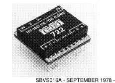
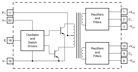
The 722 converts a single 5VDC to 16VDC input into a pair of bipolar output voltages of the same value as the input voltage. The converter is capable of providing a total output current of 64mA at rated voltage accuracy and up to 200mA without damage. The two output channels are isolated from the input and from each other. They may be connected independently, in series for higher output voltage or in parallel for higher output current, as a single channel isolated DC/DC converter. Integrated circuit construction of the 722 reduces size and cost. High isolation breakdown voltages and low leakage currents are assured by special design and construction that
includes use of a high dielectric strength, low leakage coating used on the internal assembly. A self-contained 900kHz oscillator drives switching circuitry, which is designed to eliminate the common problem of input current spiking due to transformer saturation or crossover switching.
Please be aware that an important notice concerning availability, standard warranty, and use in critical applications of Texas Instruments semiconductor products and disclaimers thereto appears at the end of this data sheet.
Copyright © 2003, Texas Instruments Incorporated
PRODUCTION DATA information is current as of publication date. Products conform to specifications per the terms of Texas Instruments standard warranty. Production processing does not necessarily include testing of all parameters.
Page 2
PACKAGE/ORDERING INFORMATION
| PRODUCT | PACKAGE-LEAD | PACKAGE DESIGNATOR(1) | SPECIFIED TEMPERATURE RANGE(2) | PACKAGE MARKING | ORDERING NUMBER | TRANSPORT MEDIA, QUANTITY |
| 722 722BG 722MG | DIP-20 DIP-20 DIP-20 | JND JND JND | –25°C to +85°C –25°C to +85°C –25°C to +85°C | 722 722BG 722MG | 722G 722BG 722MG | Rails, 17 Rails, 17 Rails, 17 |
NOTES: (1) For the most current specifications, and package information, refer to our web site at www.ti.com. (2) –25°C to +60°C for 16mA ≤ ILOAD ≤ 40mA per output.
ABSOLUTE MAXIMUM RATINGS(1)
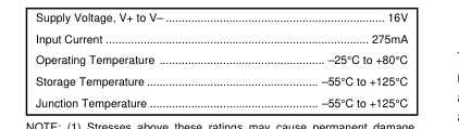
NOTE: (1) Stresses above these ratings may cause permanent damage. Exposure to absolute maximum conditions for extended periods may degrade device reliability. These are stress ratings only, and functional operation of the device at these or any other conditions beyond those specified is not implied.
ELECTROSTATIC
DISCHARGE SENSITIVITY
This integrated circuit can be damaged by ESD. Texas Instru-
ments recommends that all integrated circuits be handled with
appropriate precautions. Failure to observe proper handling
and installation procedures can cause damage.
ESD damage can range from subtle performance degradation
to complete device failure. Precision integrated circuits may be
more susceptible to damage because very small parametric
changes could cause the device not to meet its published
specifications.
Page 3
ELECTRICAL CHARACTERISTICS
At TA = +25°C, VIN = 15VDC, C = 0.47µF, and R1 selected per typical characteristic, unless otherwise noted.
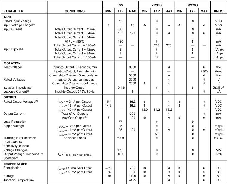
✽ Specifications same as 722. NOTES: (1) For ambient temperature above +70°C, the input voltage is 12.5V (max). The input voltage remains 16V (max) if case temperature is kept below +85°C. (2) External capacitor across P+ to V– pins and 12" of #24 wire to VIN. (3) Reference UL544, paragraph 27.5, Leakage Current. (4) See Typical Characteristics. (5) A minimum output current of 3mA at each output is recommended to maintain output voltage accuracy.
Page 4
TYPICAL CHARACTERISTICS
At TA = +25°C, VIN = 15VDC, C = 0.47µF, and R1 selected per typical characteristic, unless otherwise noted.
SELECTION OF R1 OR EXTERNAL VOLTAGE V+
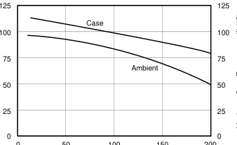
MAXIMUM SAFE OPERATING TEMPERATURE
FOR MINIMUM INTERNAL POWER DISSIPATION
vs TOTAL OUTPUT CURRENT
| MAXIMUM OUTPUT CURRENT FROM ANY SINGLE OUTPUT | ||||
|---|---|---|---|---|
| <16mA | 16mA to 30mA | 30mA | ||
| Input Voltage (V) | >13 | 1.3kΩ | 820Ω | 510Ω |
| 11 to 13 | 820Ω | 510Ω | 200Ω | |
| 9 to 11 | 510Ω | 200Ω | 0Ω | |
| 8 to 9 | 200Ω | 0Ω | — | |
| <8 | 0Ω | — | — | |
| V+ EXT | 6.5V | 7.5V | 9.0V | |
0 50 100 150 200
Total Output Current(2) (mA)
SINGLE-CHANNEL LOAD REGULATION
OUTPUT VOLTAGE vs INPUT VOLTAGE
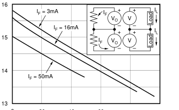
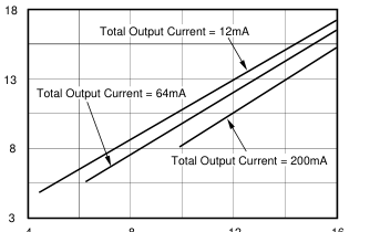
8
12
16
4
0 20
Input Voltage (V)
SINGLE OUTPUT LOAD REGULATION
40 60 80 100
Output Load Current |IL| (mA)
CHANNEL-TO-CHANNEL INTERACTION
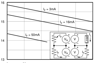
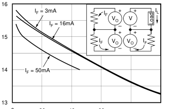
0 20 40 60 80
0
100
20 40 60 80 100
Output Load Current |IL| (mA)
Output Load Current |IL| (mA)
NOTES: (1) Using a 104mm x 19mm x 1.6mm aluminum strip mounted to the bottom of the case with heat sink compound. (2) Total output current is the sum of the currents for each individual output.
Page 5
TYPICAL CHARACTERISTICS (Cont.)
At TA = +25°C, VIN = 15VDC, C = 0.47µF, and R1 selected per typical characteristic, unless otherwise noted.
PARALLEL OUTPUT BALANCED LOAD REGULATION
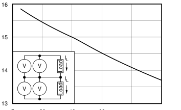
0 20 40 60 80 100
Output Load Current |IL| (mA)
PARALLEL OUTPUT UNBALANCED LOAD REGULATION
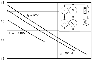
0 40 80 120 160 200
Output Load Current |IL| (mA)
OUTPUT-TO-OUTPUT INTERACTION
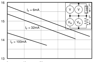
0 40 80 120 160 200
Output Load Current |IL| (mA)
Page 6
INSTALLATION AND
OPERATING INSTRUCTIONS
Typical application connections for the 722 are shown in Figures 1 and 2. Primary power (VIN) is applied at the P+ and V– terminals. The common or ground for VIN may be connected to either P+ or V–; the only requirement is that P+ and V+ must be positive with respects to V–. Power for the internal oscillator and switch drivers is derived from the primary power by a voltage dropping resistor, R1. The value of R1 as a function of VIN is shown in the Typical Characteristics section. Alternately, voltage for the V+ terminal can be obtained from a separate source. V+ should be +5V to +7.5V positive with respect to V–. If a separate source is used, the V+ input must be applied before the P+ input in
order to avoid possible damage to the unit. P+ and V+ must remain positive with respect to V– at all times (including transients). If necessary, diode clamps should be attached across these inputs. The E pin enables the converter when connected to V+ and disables it when connected to V–. An external capacitor, C (0.47µF ceramic), is used to reduce input ripple. It should be connected as close to the P+ and V– pins as practical. Input leads to these terminals should also be kept as short as possible. External shielding may be appropriate in applications where RFI at the 900kHz nominal oscillator frequency is a problem because the 722 is not internally shielded.
Each output is filtered with an internal 0.22µF capacitor. Output ripple voltage can be reduced below the specified value by adding external capacitors up to 10µF between each output and its common.
DISCUSSION
OUTPUT CURRENT RATINGS
At rated output voltage accuracy, the 722 is capable of providing 64mA divided among its four outputs(1). A minimum average output current of 3mA is recommended at each output to maintain voltage accuracy. Output channels(2) can be connected in series or parallel for higher output voltage or current.
ISOLATION CONFIGURATIONS
The fact that the two outputs of the 722 are isolated from the input and from each other allows both two-port and three-port isolation connections. Figure 1 shows TI’s 3650 optically coupled isolation amplifier connected in three-port configuration. One of the 722 channels provides power to the 3650 input. The other channel supplies power to the 3650 output. The amplifier input and output are isolated from each other and the system power supply common. In this configuration, the 722 channel-to- channel isolation specification applies to the amplifier inputto-output voltage.
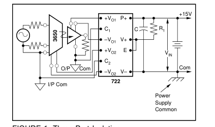
FIGURE 1. Three-Port Isolation.
NOTES: (1) “Output” denotes a single output terminal (+V or –V) and its associated common. (2) “Channel” denotes a pair of outputs (+V and –V) and their associated common.
Page 7
Figure 2 illustrates how the 722 can provide isolated input power to the input stage of two 3650s connected in the twoport configuration. Power for the output stage is provided by the system +15V and –15V supplies. Input stages are isolated from each other and from the system supply. In this situation, the 722 input-to-output isolation specification ap- plies to the amplifier input-to-output voltages, whereas the channel-to-channel 722 specification applies to the voltage existing between I/P Com #1 and I/P Com #2.
SHORT CIRCUIT PROTECTION
The circuit in Figure 3 may be added to the input of the 722 to protect it from damage in situations where too much current is demanded from the outputs—such as a short circuit from an output to its common. The circuit limits input current to approximately 150mA for an input voltage of 15VDC (for ß of 2N2219 of 50).
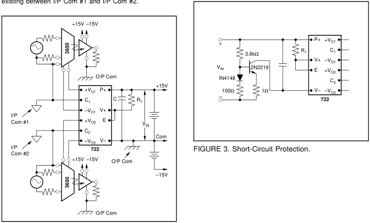
FIGURE 2. Two-Port Isolation with Two 3650s.
Page 8
PACKAGE DRAWING
JND (R-CDIP–P20)
CERAMIC DUAL-IN-LINE
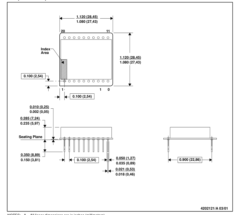
NOTES: A. All linear dimensions are in inches (millimeters). B. This drawing is subject to change without notice. C. Leads in true position within 0.010 (0,25) R @ MMC at seating plane. D. Pin numbers shown for reference only. Numbers may not be marked on package. E. A visual index feature must be located within the cross–hatched area.
Page 9
PACKAGE OPTION ADDENDUM
3-Oct-2003
PACKAGING INFORMATION

(1) The marketing status values are defined as follows: ACTIVE: Product device recommended for new designs. LIFEBUY: TI has announced that the device will be discontinued, and a lifetime-buy period is in effect. NRND: Not recommended for new designs. Device is in production to support existing customers, but TI does not recommend using this part in a new design. PREVIEW: Device has been announced but is not in production. Samples may or may not be available. OBSOLETE: TI has discontinued the production of the device.
Page 10
IMPORTANT NOTICE
Texas Instruments Incorporated and its subsidiaries (TI) reserve the right to make corrections, modifications, enhancements, improvements, and other changes to its products and services at any time and to discontinue any product or service without notice. Customers should obtain the latest relevant information before placing orders and should verify that such information is current and complete. All products are sold subject to TI’s terms and conditions of sale supplied at the time of order acknowledgment.
TI warrants performance of its hardware products to the specifications applicable at the time of sale in accordance with TI’s standard warranty. Testing and other quality control techniques are used to the extent TI deems necessary to support this warranty. Except where mandated by government requirements, testing of all parameters of each product is not necessarily performed.
TI assumes no liability for applications assistance or customer product design. Customers are responsible for their products and applications using TI components. To minimize the risks associated with customer products and applications, customers should provide adequate design and operating safeguards.
TI does not warrant or represent that any license, either express or implied, is granted under any TI patent right, copyright, mask work right, or other TI intellectual property right relating to any combination, machine, or process in which TI products or services are used. Information published by TI regarding third-party products or services does not constitute a license from TI to use such products or services or a warranty or endorsement thereof. Use of such information may require a license from a third party under the patents or other intellectual property of the third party, or a license from TI under the patents or other intellectual property of TI.
Reproduction of information in TI data books or data sheets is permissible only if reproduction is without alteration and is accompanied by all associated warranties, conditions, limitations, and notices. Reproduction of this information with alteration is an unfair and deceptive business practice. TI is not responsible or liable for such altered documentation.
Resale of TI products or services with statements different from or beyond the parameters stated by TI for that product or service voids all express and any implied warranties for the associated TI product or service and is an unfair and deceptive business practice. TI is not responsible or liable for any such statements.
Following are URLs where you can obtain information on other Texas Instruments products and application solutions:
Products
Applications
Amplifiers
amplifier.ti.com
Audio
Data Converters
dataconverter.ti.com
Automotive
DSP
dsp.ti.com
Broadband
Interface
interface.ti.com
Digital Control
Logic
logic.ti.com
Military
Power Mgmt
power.ti.com
Optical Networking
Microcontrollers
microcontroller.ti.com Security
Telephony Video & Imaging Wireless
Mailing Address: Texas Instruments
Post Office Box 655303 Dallas, Texas 75265
www.ti.com/audio www.ti.com/automotive www.ti.com/broadband www.ti.com/digitalcontrol www.ti.com/military www.ti.com/opticalnetwork www.ti.com/security www.ti.com/telephony www.ti.com/video www.ti.com/wireless
Copyright 2003, Texas Instruments Incorporated