
DATASHEET SEARCH SITE
Document overview
- Manufacturer or author: Provided By digicamel.com
- PDF pages: 12
Technical content
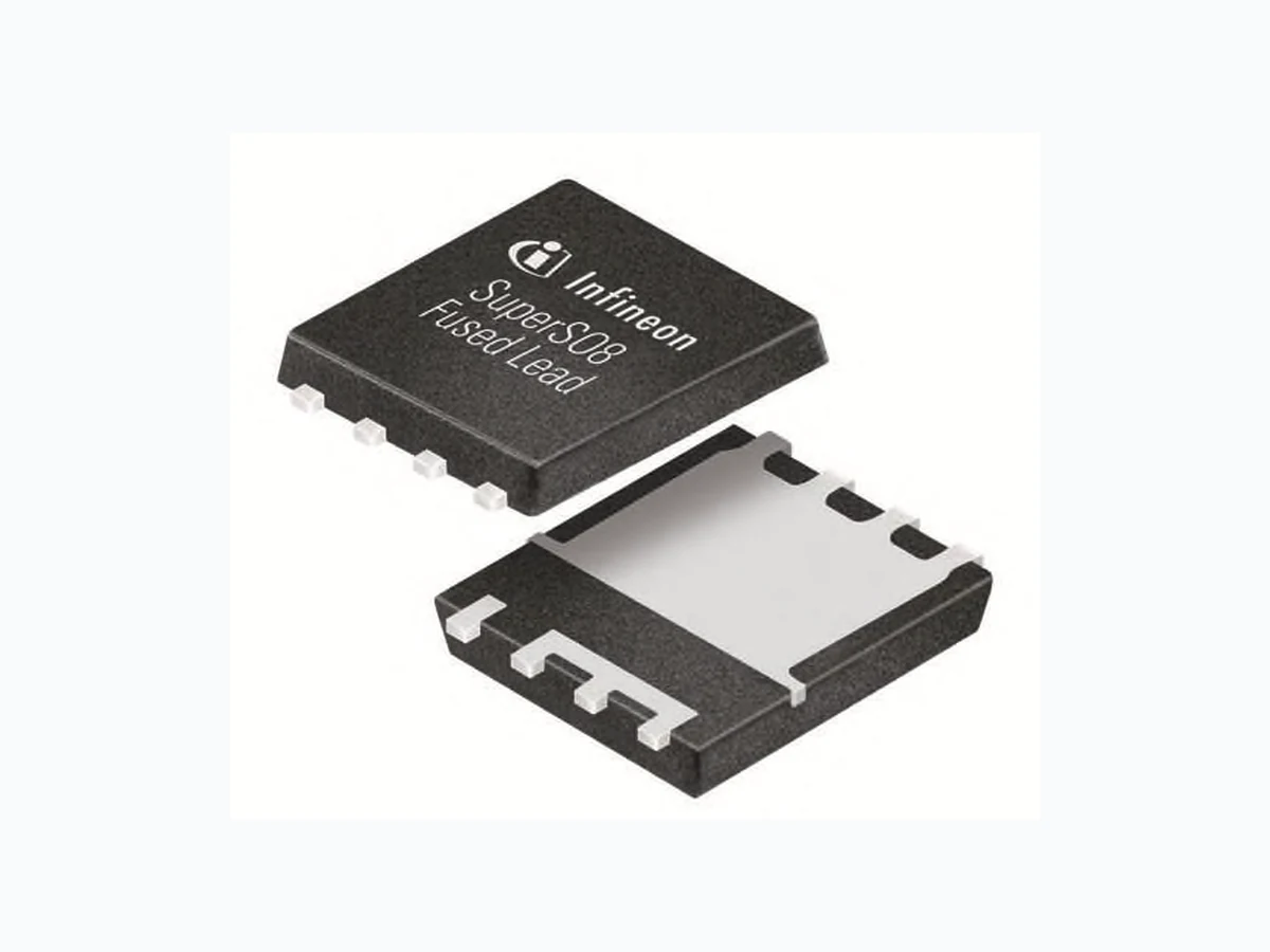
OptiMOS™ 5 Power-Transistor, 30 V ITDSON-8 FL (enlarged source interconnection)| Features <j A + Very low on-resistance Rosjon) @ Ves=4.5 V * Optimized charges for fast switching 4 5 + Optimized QGD/QGS for induced turn on ruggedness 23 ~ 7 + Superior thermal resistance Y Sa + N-channel + 100% avalanche tested bie, + Pb-free lead plating; ROHS compliant 2 + Halogen-free according to IEC61249-2-21 ‘ Product validation Fully qualified according to JEDEC for Industrial Applications st 7] [- 6D s2 7] (=3) fj 7D Table 1 Key Performance Parameters $3 al (No [F 6D @ RoHS BSCOOSNO3LS5 PG-TDSON-8 FL O5NO3LS5 [le Final Data Sheet 1 Rev. 2.1, 2020-12-22
OptiMOS™ 5 Power-Transistor, 30 V Cinfi neon BSCOO5NO3LS5 Table of Contents Final Data Sheet 2 Rev. 2.1, 2020-12-22
OptiMOS™ 5 Power-Transistor, 30 V nrineon BSCOO5NO3LS5
1 Maximum ratings
at Ta=25 °C, unless otherwise specified Table 2__ Maximum ratings Paramet ymeot [—taues Note / Test Condit arameter [Min. | ote / Test Condition Typ. Max. |
433 Ves=10 V, Tc=25 °C
. A Voes=10 V, Tc=100 °C 1) (os » Te’ Continuous drain current Io 306 A Vos=4.5 V, Ta=25 °C, Rra=50 °C/W?) Pulsed drain current? lioowe (- - 1731 Ta=25 °C Avalanche energy, single pulse® les |- ——si|- ——[g00. mu _ | Ip=50 A, Ros=25 Q sci tt 188 Tc=25 °C Power dissipation me EF pe he | Ta=25 °C, Rrnia=50 °C/W? . ° IEC climatic category; DIN IEC 68-1:
2 Thermal characteristics
Table 3 Thermal characteristics Paramet mea [ae Note / Test Condit arameter ote / Test Condition [min._|Typ. [Max._| Thermal resistance, junction - case, ° bottom oc | fae ow - wel resistance, junction - case, oc |} Fao ow . Device on PCB, ° 6 cm? cooling area Fon Fo. *) Rating refers to the product only with datasheet specified absolute maximum values, maintaining case temperature as specified. For other case temperatures please refer to Diagram 2. De-rating will be required based on the actual environmental conditions. 2) Device on 40 mm x 40 mm x 1.5 mm epoxy PCB FR4 with 6 cm? (one layer, 70 ym thick) copper area for drain connection. PCB is vertical in still air. 3) See Diagram 3 for more detailed information ” See Diagram 13 for more detailed information Final Data Sheet 3 Rev. 2.1, 2020-12-22
OptiMOS™ 5 Power-Transistor, 30 V ¢ In Ineon BSCO05NO03LS5 3_ Electrical characteristics at Tj=25 °C, unless otherwise specified Table 4 Static characteristics Parameter Symbol [Min. | T wx Note / Test Condition Drain-source breakdown voltage [Veaoss [30 |- |- |v | Ves=0 V, lb=1 mA Gate threshold voltage Vos=Ves, 250 HA Zero gate voltage drain current lees | oo to0 ye35 Vv ay My pat3s sc Gate-source leakage current licss [= ——«|10—s[t00. [na Ves=20 V, Vos=0 V - a 0.48 {0.55 Ves=10 V, Ib=50 A Drain-source on-state resistance roam [ R&BES Ima | Ves=4.5 V, Ib=50 A Transconductance lo «[- ——if300 *[- Ss [Vos|22|/o|Ros(on)max, Ib=50 A Table 5 Dynamic characteristics Parameter oo T wax Note / Test Condition Input capacitance [Css [= —«[8900 |- [pF __ | Vas=0 V, Vos=15 V, 1 MHz Output capacitance [Con [= «(2700 |- [pF | Vas=0 V, Vos=15 V, fe1 MHz Reverse transfer capacitance [Case (300 - Spe Ves=0 V, Vos=15 V, f1 MHz Turn-on delay time eee pels Me foon4s V, b=50 A, ise ti Voo=15 V, Ves=4.5 V, Ib=50 A, Tum-off delay time luon | faa os | Voor BV, Vos=4.5 V o=50 A, . Vop=15 V, Ves=4.5 V, /n=50 A, Table 6 Gate charge characteristics” Parameter sym T wos | Note / Test Condition Gate to source charge [ase 2t|- [nC _ | Von 18 V, fo=50 A, Vos=0 to 4.5 V Gate charge at threshold [Quem - —*12 + |n_| Von= 48 V, fo=50 A, Vos=0 to 4.5 V Gate to drain charge [Qe Et |r| Von 45 V, fo=50 A, Vos=0 to 4.5 V Switching charge [Qw [= ——«22—|- [nC _ | Von V, fo=50 A, Vos=0 to 4.5 V Gate charge total la Ef + |r| Von 15 V, fo=50 A, Vos=0 to 4.5 V Gate plateau voltage [Vows (23 |_| Von 45 V, 0-50 A, Vos=0 to 4.5 V Gate charge total la ft22 + nc Von 45 V, b=50A, Vos=0 to 10 V ») Defined by design. Not subject to production test. 2) See "Gate charge waveforms” for parameter definition Final Data Sheet 4 Rev. 2.1, 2020-12-22
OptiMOS™ 5 Power-Transistor, 30 V ¢ In ineon BSCO05NO03LS5 Table 7 Reverse diode Paramet symbol Note / Test Condit arameter ymbo! [min. | ote / Test Condition Hyp. [Max Diode continuous forward current lis (- i[- ——s[taa [A Tc=25 °C Diode forward voltage [Vo |- «0.79 [4 |V__| Vas 0 V, =50 A, Ti=25 °C Reverse recovery charge la |- —fg0s/ Sn Va=15 V, Ir=Is, dir/dt=400 A/yus Final Data Sheet 5 Rev. 2.1, 2020-12-22
OptiMOS™ 5 Power-Transistor, 30 V ¢ In fi neon BSCOOSNO3LS5 0
4 Electrical characteristics diagrams
a 15 a a es \\ ep \\ a 150 eS a a 125 soo |) eS z e = 100 . a a a é a a \\ 200} Nr 75 a \\ a \\ a 50 a \\ Se a a 25 \\ SV a a a 0 a 0 25 50 7 100 125 150 175 200 0 25 50 75 100 125 150 175 200 Te [°C] Te PC] EEE SSS StH H—- sor RAPE eH a []--- 0.02 eee COLE St CTT Hew 0.05 TTI COTTE COT COT
10 SSS SS aa | ae ee
Seneca sel |. eccl UMIIT ZEISS Ce Oe ee ee ve ZINA TN ieee ETT eile mestt eet cilia =a Se |S Coe sem Cr CC = SSAC SSS SHES tmnt = rome oj re on fe GUT TT * Se | MATT 10° Ly TT Te a ll Creer ecco =a SS OCs Sere 2040 A ee eesti ii PZT CE TI PET AT CREE NT oe ETI TTT TTT TTT wo + LUO TE IN TTY] age Vos IVI ts] Final Data Sheet 6 Rev. 2.1, 2020-12-22
OptiMOS™ 5 Power-Transistor, 30 V ¢ In neon BSCO05NO03LS5 jiagram 5: Typ. output characteristics jiagram 6: Typ. drain-source on resistance Di T, hi isti Di 6: Typ. draii i 1750 i 190 T7728 VED HEHE EEE HOARE EEE sv /| /\\/ Dee mere a, 1500 / y UF 105 ZAC) Sle” 74 V COCOA CCC eee VV K| COOAEC CCC A 1250 / a? 400s | WV y 1.00 ACEC eee 0 a If EEEEEE EEE EEEEEEEEH EE / = = eT POC 2 eee ea < Foo 7s COLL CCCCCee 2 ts ee LW Vat & a eee eel
750 IA é Beer ees v
a f oso Ee oo YY. © PREEPEE EEE EEE WA | EERE EEE EEE / i WY MTEL TTT os LOCOCO
280 Fo BV Sg
Ys ; a Y; a | (| a | of 0.00 OCCA err Vos [V] Io IA] Ib=f(Vos), Ti=25 °C; parameter: Ves Rosion=t(lo), T=25 °C; parameter: Vos Diagram 7: Typ. transfer characteristics Diagram 8: Typ. drain-source on resistance 1780 [75°C 1.50 eee EEE bee | /| |
1500 Wry 45 COCCCECE CCC)
| Se |
1250 Se |
/ 100 COCCCECAC CCS) dg EEEEEEER EERE Prs-oS 4000 [| f > COCCCCeC eee a = // g | < Fos COE 2 oe A / & 2 Ne 750 / é ee eee S000 SSeS 7p / 0.50 LE ECCCCee rrr ee / lg 500 a | y, a | /] a | Vj eee 250 4 lg 7 a a | y 4 a | 0 ay 0.00 OCCT 0 1 2 3 4 5 0 2 4 6 8 10 Ves [V] Ves [V] Io=f(Ves), |Vos|>2|/o|Ros(onmax; parameter: T) Roston)=f(Ves), lo=50 A; parameter: Tj Final Data Sheet 7 Rev. 2.1, 2020-12-22
OptiMOS™ 5 Power-Transistor, 30 V ¢ In neon BSCOOS5NO3LS5 Diagram 9: Normalized drain-source on resistance Diagram 10: Typ. gate threshold voltage 2.0 24 PTT TTT TT) LTT TTT TTT TT TT TT COCCI LTT TTT ee ee COCCI LTT TTT LA cot TTT TTT se HTT Pt <2 OS LITT TTT TT TTT Pr TT COCO ° mT Correo | ES 2 12 YO LET TTT TT PNP
3 WTA COC PS PSS
8 WW = S S
L 4 & ” N N E ChELDEeTTLELEELEELELELEELELLE |S LEP TTT ENON E oe ea | 2 87 PeTLELLLELLL ELLE EEL ELL LTT TTT TN EIN TTT SCO oe EEN “LOTT TTT TTT TT PE 4 04 COCO HEE HE He =e LTT TTT ee et LETT TTT TTT CCEA) ne -80 -40 0 40 80 120 160 200 -80 -40 0 40 80 120 160 200 Teel Teel Roson=f(T1), lb=50 A, Ves=10 V Diagram 11: Typ. capacitances 10° eee eee 10" qe SEE SEEDS SSS ESS Sse esse se Sesaee Hoos PDE Se Se Sees See ea 25°C FREESE SEE EEE EEE EEE EEE H HERR R EEE EEE EEE CePrr rrr errr eer eee eee eee) [}— — 25°C, max FOr CEPT yr terre re reer [}--= 175°C rrr rrr ye eee LETT T TT TTT Tt [J----- 175°C, max | TT TTT TTT TTT TTT TTT CTT STAATOHUATAATOVOTENTOATODSezz ee UIT) | TTT EP NaF EE DEE EE EE EE EEE iss See eee ae ESSER SEER EE EEE EEE PERE EEEEEEEEEE eee Coromreeeeeeeeeeeeeeeeeeeeeeeeeeeeeeee Cerra Cc CEPT SSD = ey ea & HTT =< LE eA eT ° SH * HH ee eee w NUTT Te |. LOTTA TT SENSI ESSE Se eee See eee sce ESas =B es Scoh ee pee cue cesece ce TERNS SSS SEES SEE SESE SSIS ESSE ESRC RSE SUSIE ESS COPS) ee Bee BA 2 CEPT TT See Oe ee HTT Ha CET re | LOTTE TUTTE) PTET Fil it 10° 10° Vos [V] Vso [V] C=f(Vos); Ves=0 V; 1 MHz Final Data Sheet 8 Rev. 2.1, 2020-12-22
e" fi OptiMOS™ 5 Power-Transistor, 30 V In neon BSCOOSNO3LSS Diagram 13: Avalanche characteristics Diagram 14: Typ. gate charge A nn i 10 z _— | [7 TUTTI TTT TT TT TT TTT Tr HT 6 COOP a A a | | —-15V TELLELEEE LEELA SHENTON | SERRE CCCI FPPC SMSC | EEREEEEEEEEEEEEE AHP DN IN HIN ye UTIL TIN UIIN 2h | FEEEEEEEEEEE aA 10) {NS 40 SETS ErT PNR | COPECO a fT 2 ae > CTT Cn 00 °c S CECEELCLLELEL EL CEE =< LOTT Pn TINT < COOCCELEL ae
2 CUI TUITE TUTTI NUT $0 ESE er
to EL 80° LTT a Besar sett sere EERE EEE EEE eH et aoy 20 24Gn 0S CTT TP 2 HAE COC Fe Coc Co EAE 10° rp 48 oe 10° 10° 10° 10° 10° 0 25 50 75 100 125 tav [Hs] Qgate [NC] Ins=f(tav); Res=25 Q; parameter: Tjstat Vos=f(Qoate), lo=50 A pulsed, T=25 °C; parameter: Voo Diagram 15: Drain-source breakdown voltage Diagram Gate charge waveforms 3 eee ne ee | Vos ste CYT TT Try rr aA Q Re ey ee g ey ee Ee ee soft eee CYT TT rrr ry ry ty ee Re ee = CYT TT rrr ry rrr yr s set ee
8 CYT TTT rr yt A
CYT ATT re ) Soon Rom | | Oe Q gare CPA TTT ere CYTA TUT re Pee | Qou 0 40 0 40 80 120 160 200 TPC] Venoss TT A _ Final Data Sheet 9 Rev. 2.1, 2020-12-22
OptiMOS™ 5 Power-Transistor, 30 V nrineon BSCO05NO03LS5
5 Package Outlines
D Le | J | | WWI | ns - a uw ws | Td b 7 \\ [> [aaa@ [A] Z iy z | 4 | ole ol =| [ZJeee|2] [wumerers [INCHES DOCUMENT NO. [win Tmax TNT 28800162237 [a oo to os ona [AS 05 (RER) OTT REF) | scale © a [er oe ze ocor 008 | 25 Poo BSC) 0208(880) [or S00 Sc) TST BSC) 9 uk yc | "5mm Sa A [er |___s.o0 es) 0286850) ) Ss egropcan pRovECTION [ee sao aoe to [—e| ares) CCST C* a OO a XOX | [oe ose os ae ISSUE DATE [a ats 5 ore ora 02-08-2011 [RT oases Tore 0023 [aaa oot REVISION [eco [008 00 7 ot Figure 1 Outline PG-TDSON-8 FL, dimensions in mm/inches Final Data Sheet 10 Rev. 2.1, 2020-12-22
Figure 2. Outline Boardpads (TDSON-8 FL)
—_— I fi OptiMOS™ 5 Power-Transistor, 30 V nrineon BSCOO5NO3LS5
Revision History
Revision: 2020-12-22, Rev. 2.1 Previous Revision Revision [Date __| Subjects (major changes since last revision) 2.0 2020-04-16 | Release of final version 2.1 2020-12-22 |Update Id for VGSTH Trademarks All referenced product or service names and trademarks are the property of their respective owners. We Listen to Your Comments Any information within this document that you feel is wrong, unclear or missing at all? Your feedback will help us to continuously improve the quality of this document. Please send your proposal (including a reference to this document) to: erratum@infineon.com Published by Infineon Technologies AG
81726 Miinchen, Germany
© 2020 Infineon Technologies AG All Rights Reserved. Legal Disclaimer The information given in this document shall in no event be regarded as a guarantee of conditions or characteristics (‘Beschaffenheitsgarantie’) . With respect to any examples, hints or any typical values stated herein and/or any information regarding the application of the product, Infineon Technologies hereby disclaims any and all warranties and liabilities of any kind, including without limitation warranties of non-infringement of intellectual property rights of any third party. In addition, any information given in this document is subject to customer's compliance with its obligations stated in this document and any applicable legal requirements, norms and standards concerning customer's products and any use of the product of Infineon Technologies in customer's applications. The data contained in this document is exclusively intended for technically trained staff. It is the responsibility of customer's technical departments to evaluate the suitability of the product for the intended application and the completeness of the product information given in this document with respect to such application. Information For further information on technology, delivery terms and conditions and prices please contact your nearest Infineon Technologies Office (www.infineon.com). Warnings Due to technical requirements, components may contain dangerous substances. For information on the types in question, please contact the nearest Infineon Technologies Office. The Infineon Technologies component described in this Data Sheet may be used in life-support devices or systems and/or automotive, aviation and aerospace applications or systems only with the express written approval of Infineon Technologies, if a failure of such components can reasonably be expected to cause the failure of that life-support, automotive, aviation and aerospace device or system or to affect the safety or effectiveness of that device or system. Life support devices or systems are intended to be implanted in the human body or to support and/or maintain and sustain and/or protect human life. If they fail, it is reasonable to assume that the health of the user or other persons may be endangered. Final Data Sheet 12 Rev. 2.1, 2020-12-22