
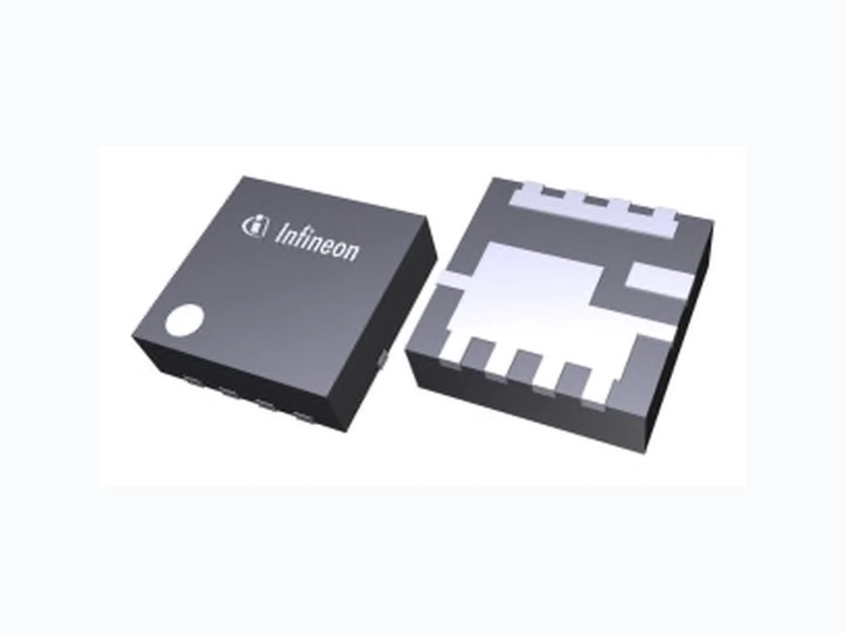
IQE050N08NM5CG INFINEON
Document overview
- Manufacturer or author: Provided By digicamel.com
- PDF pages: 12
Technical content
OptiMOS™ 5 Power-Transistor, 80 V PG-TTFN-9-1 Features an * Optimized for synchronous rectification + Very low on-resistance Rosjon) ° + 100% avalanche tested + Superior thermal resistance rn 7 + N-channel, normal level a4 a, + Pb-free lead plating; ROHS compliant + Halogen-free according to IEC61249-2-21 Product validation Fully qualified according to JEDEC for Industrial Applications rain Pins Table 1 Key Performance Parameters om Pin 4 [Rosenman 5.0 me a @ @ RoHS IQEOSONO8NMSCG PG-TTFN-9-1 osooscs =| Final Data Sheet 1 Rev. 2.0, 2021-04-26
OptiMOS™ 5 Power-Transistor, 80 V Cinfi neon IQEO50N08NM5CG Table of Contents Final Data Sheet 2 Rev. 2.0, 2021-04-26
OptiMOS™ 5 Power-Transistor, 80 V nrineon IQEO50NO8NM5CG
1 Maximum ratings
at Ta=25 °C, unless otherwise specified Table 2__ Maximum ratings Paramet ymeot [—taues Note / Test Condit arameter [Min. | ote / Test Condition Typ. Max. |
101 Ves=10 V, Tc=25 °C
Continuous drain current’? lo 11 A Ves=10 V, Tc=100 °C »)
16 Ves=10V, Ta=25°C, Rinsa=60°C/W'
Avalanche energy, single pulse les |e |- [t84 fms Ip=20 A, Res=25 Q «cin at 100 Tc=25 °C Power dissipation me Eb fF pe bh | Ta=25 °C, Roua=60 °C/W? Operating and storage temperature ite [ss | is fo | re cumatic category; DIN IEC 68-1:
2 Thermal characteristics
Table 3 Thermal characteristics Paramet symbol Note / Test Condit arameter ymbol [Min. | jlote / Test Condition Tye. Max. | Thermal resistance, junction - case, ey bottom roc | fos fis tow : Device on PCB, ° 6 om? cooling area ow Feo bow. *) Rating refers to the product only with datasheet specified absolute maximum values, maintaining case temperature as specified. For other case temperatures please refer to Diagram 2, De-rating will be required based on the actual environmental conditions. 2) Device on 40 mm x 40 mm x 1.5 mm epoxy PCB FR4 with 6 cm? (one layer, 70 ym thick) copper area for drain connection. PCB is vertical in still air. 3) See Diagram 3 for more detailed information ” See Diagram 13 for more detailed information Final Data Sheet 3 Rev. 2.0, 2021-04-26
OptiMOS™ 5 Power-Transistor, 80 V ¢ In Ineon IQEO50N08NM5CG 3_ Electrical characteristics at Tj=25 °C, unless otherwise specified Table 4 Static characteristics Parameter Symbol [Min. | T wx Note / Test Condition Drain-source breakdown voltage [Venoss 80 |- |- |v | Ves=0 V, lb=1 mA Gate threshold voltage Vos=Ves, lo=49 WA Zero gate voltage drain current lees | oo 1a yesn85 Vv ay My pat3s sc Gate-source leakage current licss [= ——«|10—s[t00. [na Ves=20 V, Vos=0 V . . 4.3 5.0 Ves=10 V, Ib=20 A Drain-source on-state resistance From F838 Ime | Ves=6 V, lo=5 A Transconductance lo. [38s 75> Ss [Vos|22|/o|Ros(on)max, Ib=45 A Table 5 Dynamic characteristics Parameter oo T wax Note / Test Condition Input capacitance” [Css —(-__[2200_[2900 Ves=0 V, Vos=40 V, f=1 MHz Output capacitance") [Con (= ——«([370.—([480 [pF Ves=0 V, Vos=40 V, 1 MHz Reverse transfer capacitance” [Cos e237 [pe Ves=0 V, Vos=40 V, f1 MHz Turn-on delay time eee pea Me fosrt0 V, b=20 A, ise ti Vov=40 V, Ves=10 V, In=20 A, i Vov=40 V, Ves=10 V, Io=20 A,
7 Voo=40 V, Ves=10 V, p=20 A,
Table 6 _Gate charge characteristics” Parameter sym T wos | Note / Test Condition Gate to source charge [Qs [- «40.0 |- [nC _| Vo=40 V, 1o=20 A, Vos=0 to 10 V Gate charge at threshold lam |- jaz |- [nc | Voo=40 V, In=20 A, Ves=0 to 10 V Gate to drain charge” [Qe Fs |8.8 [43 [nC | Von=40 V, b=20A, Vos=0 to 10 V Switching charge [Qwest = [nC _ | Von 40 V, fo=20 A, Vos=0 to 10 V Gate charge total” la, se ——|34.6 [43.2 nC | Voo=40 V, fo=20 A, Vos=0 to 10 V Gate plateau voltage [Vows (4.8 |V [Von 40 V, f0=20 A, Vos=0 to 10 V Gate charge total, sync. FET [Qsemy |- «2a |- |r| Vos=0.1 V, Ves=0 to 10 V Output charge” [asf f4ofs3_ nc |vos=40 v, Vasr0V ” Defined by design. Not subject to production test. 2) See "Gate charge waveforms” for parameter definition Final Data Sheet 4 Rev. 2.0, 2021-04-26
OptiMOS™ 5 Power-Transistor, 80 V ¢ In fi neon IQEOSONOBNMSCG Table 7 Reverse diode ‘arameter yymbol jote esi ondition [min [Typ.[Max._| Diode continuous forward current ls | |- (7 [a | Tc=25 °C Diode pulse current [sows [> [aoe fA [To 25 °C Diode forward voltage [Vo |= ——(f0.83 [4.4 |V | Ves=0V, Ik=20 A, T=25 °C Reverse recovery time’? lt |- —'|a7_—s[7a— [ns Va=40 V, Ir=20 A, dic/dt=100 A/us Reverse recovery charge” las |- «8060 [nC | Va=40V, fe=20 A, dir/dt=100 Als Defined by design. Not subject to production test. Final Data Sheet 5 Rev. 2.0, 2021-04-26
OptiMOS™ 5 Power-Transistor, 80 V ¢ In neon IQEO50NO8NM5CG
4 Electrical characteristics diagrams
Diagram 1: Power dissipation Diagram 2: Drain current 120 [rr rr i a a a a a a a a oo _—=_ rrr rr ES Se a a SS a a a A eS | 99 a a a a a AS | SS a a Fo oN E —=g SN 3 a Cn a a SG a eS a A A a a | S| a | TS SS | a NS SG a SS a SS | 29 SS SS SO RW eS | a a a A | a a a es | a a A a a a 0 25 50 75 100 125 150 175 200 i) 25 50 75 100 125 150 175 200 Te [°C] Tc [°C] Po=t(To) To=l(To); Ves=10 V Diagram 3: Safe operating area Diagram 4: Max. transient thermal impedance
0 SS ae 10) | See
=a ee H— singe pulse HHH FFE FF EEA oo []— 0.01 noo on HHS |S te 1 et fet = ae [ea || SHH ett |” RT se | vor OLE DNs UT SS ee Se == eee | Comet =< ee ete A a Ere CCI CTT Co
2 POTHIICTTTTTINSSTTT game UTM TTT TTT TTT
+ tee Cr ICI TI LI a ae Ee es yf EERE NEE 10" AN vo LIT TANT Aono Eee Foca ned LT Tm TI TTT) ee et ee a FETE AE] ge {ETI TT TTT TTT yor — LI TE TE], 10" 10° 10° 10? 10° 10+ 10° 107 107 10° Vos [V] & [s] lp=f(Vos); Tc=25 °C; D=0; parameter: fp Zinsc=f(t); parameter: D=t)/T Final Data Sheet 6 Rev. 2.0, 2021-04-26
OptiMOS™ 5 Power-Transistor, 80 V ¢ In fi neon IQEO50NO8NM5CG 400 14 COTY I wo EE a === —— “CTT | «Se ffi 10 a 2 oo ELEY a COA ee ef att a ===eSSS= 2 [/\\ & = = = wo TCU a —— le Oe == —— 50 / ——— Hy sa p==——— BV) eo TT a YC a CC CO |
0 Beer #8 Ee
0 1 2 3 4 5 (0) 25 50 75 100 125 150 175 200 Vos [V] ofA] 350 14 THOTT) | EEEEESEe vee ECEECEECEECEECCECEETETTEA | BEPPEEREEEEPEREEEEEEEEE 2 ee ee CECCEEEEEEECCECEECEECETT HP) EEEEEEEEESE eRe vow CETTE) |g PEPPERS ESSE CECCECEEEECECEECEECEECE) | EEEEEEEEES EES woe CCEECEECTECEECCEEETE PV |. EEPPEEPEEEEEREEEE PEEP raeesUUAUAVSEAOHUOEUOENORUOINY/G00m Sal ceceeeeeuusun\\'esesesaeuee = LLL}, Ree HH) SCAT COTT) & ° EEEEEEEEE SESE je AEECECEECEECEECEETEECATTT] |} EEEEEEERECEEREr Pre b STCEEECECCATTEEE PETE)“ EEEEEEEEE EEE +0 HHT HACC 9 EEE EEE E+] MNOOEOOUUUUULUUEVY AMANO sts ccecst teed toca
0 PETE ea LET of LTT Tir ry rrr yr yy ry rer rr |
0 1 2 va i 5 6 7 0 2 4 Ves 1 6 8 10 Final Data Sheet 7 Rev. 2.0, 2021-04-26
——. OptiMOS™ 5 Power-Transistor, 80 V ¢ In fi neon IQEO50NO8NM5CG 24 4.0 LTT TTT TTT TTT TT TT TTT LTTE) LUTTE TTT COCECECEEC Eee HEE FECEECE EEE eee er SSTTRRRERATEEP
20 PSTN
etesentontazentonsedes/catat i MMCCOa aH nAHaiiasS4t<SUAMAATALEAL o / PNK ° TTT TT TT TTT TT er SN Fab feseaeet cosa tececcHest essed MEarettT TCOMTTT AAA ae ecQGttTE a . = 7 DN IN CUT T TTT TT Arr x C | Rggrientasetense]scustenteceteail car faa Hat faataat tan aaneesoey E COO eres 32 NS oa rtaase recdtaatesetaat estas MCAT TaaH Hal taataataitaattactea = . 9 pA g 08 CORTE ECEEEEECEEELLLEE LLL pipe rosfestesteateuetarsustssscsil MCOTGAVGGHHAINAAIGLHOAEGATOAIGL PTT TTT TT Sisasarazensesetonentaterssret Ml MCCOGGTATaTaHaaHaTaTannatatatenl LUTTE TTT oo LOEEEEEC PELE 7} oo LUTE TT -80 -40 0 40 80 120 160 200 -80 -40 0 40 80 120 160 200 TPC) TPC) ° SESS SES SSSSSeeSsy | PRES RE SESS =====]=========— ippecpmiiiiniiiitisrn: A OO [}--- 175°C LrTr rrr yee Efi peppery ey ye ee []-++++ 175 °C, max HT ert N SC HEH HHP tte STS) | Te
0 SE ERS SEES SEES SSS | GREREREE REE EE RE EAEE EEE
| HERE EEE EEE EE EEE Cc NG a _ Ee Be eee & LK TT tT ee et | is LEE aT
6 ONCE ree =
LUNE EEL) |} ETT (BES SSS SSS SSS | EERREEREEE REE ESSE a | ce ee | a Ee Pe eee a SO LEP eT CECE EASE COCOA ELLE LLL ere |, IU wo [es[ TTT] | i Vos [V] Vso [V] Final Data Sheet 8 Rev. 2.0, 2021-04-26
OptiMOS™ 5 Power-Transistor, 80 V ¢ In fi neon IQEO50NO8NM5CG Diagram 13: Avalanche characteristics Diagram 14: Typ. gate charge 108 errr 107 ———= st — ee eee [= CTTITITITIIITIII — ae —isv rr a SH A A | —-40V rrertstltfrtttltttltfthO4 Co er Ho== 64 VE A FERC eee | i 2 Nl Nil NU 92 . atl ONY a wscempscrmseres | CCT er S S A et St PS Sa 4? > a A DS S FEEELELELLLIivaAcLt_eteil SEE AHHIEEPSNIP Proof Ee
2 LUA TTT I I 8 Corer eee
~ oe a a ibovc [TT Try tT ttt te et re Et HH a SS | CCAR aS SH y a ope a PA a ee 2 LT TE TE TTT HAT {ttt fy ff Tt a 2 10° of TTT Try ry ttt tt 10° 10° 107 10° 0 4 8 12 16 20 24 28 32 tav [us] Qeate [NC] Ins=f(tav), Ros=25 Q, parameter: Thwan Ves=f(Qoate), 10=20 A pulsed, 7/=25 °C, parameter: Voo Diagram 15: Drain-source breakdown voltage Diagram Gate charge waveforms CECE ECE CEE EEE eee ECE EEE CCE ECE EEE CCE Ves COCEEE ECC eee Q ee @ COCR EEE CCE eR a ea COCCCCCCCC er COCA ECA Py a eo ey a a er Pe g COCEECE CCE Ae a & eee ee eo CECCCCCC Aer} COCA SoReal COCCCCC AAR COCCCCAAC eee ye COCOA eer Sey 40 o Oey 4c Rom | | Oe Q gare COA COAEEC ECE eee eee
0 Qua
TPC] Vencss At mA OO Final Data Sheet 9 Rev. 2.0, 2021-04-26
OptiMOS™ 5 Power-Transistor, 80 V ¢ Infi neon IQEOSONOSNMSCG
5 Package Outlines
[=| [0] ot [=| - ~ [8] 2 A pa Ss E Bloke) Fo boo tot = TH 5 + A T — a | Hla tT SEO) TT Uti be 4 21011) wioex marine Al - STAN OFF [el b 8x [6]o1@[a[e[c] [meson [| a a Yo a [ea SCALE 10:1 Keer ee 0 1 2mm a Usui a EUROPEAN PROJECTION a ; [et 0305 a XC Ke [a 073 08 98.11.2019 Figure 1 Outline PG-TTFN-9-1, dimensions in mm Final Data Sheet 10 Rev. 2.0, 2021-04-26
OptiMOS™ 5 Power-Transistor, 80 V ¢ | n fi neon IQEOS0NO8NM5CG 1629 os 035 8x 1.059 0.595 r 4 N ig AlAs. Bit oe ood Pint 0.65, 14 4x 0.365 i oss looa Fa oars _|osis || ‘copper solder mask stencil apertures All dimensions are in units mm Figure 2 Outline Boardpad (PG-TTFN-9-1), dimensions in mm Final Data Sheet 11 Rev. 2.0, 2021-04-26
OptiMOS™ 5 Power-Transistor, 80 V ¢ | nrineon IQEOSONO8NMSCG
Revision History
Revision: 2021-04-26, Rev. 2.0 Previous Revision Revision [Date __| Subjects (major changes since last revision) 2.0 2021-04-26 |Release of final version Trademarks All referenced product or service names and trademarks are the property of their respective owners We Listen to Your Comments Any information within this document that you feel is wrong, unclear or missing at all? Your feedback will help us to continuously improve the quality of this document. Please send your proposal (including a reference to this document) to: erratum@infineon.com Published by Infineon Technologies AG
81726 Miinchen, Germany
© 2020 Infineon Technologies AG All Rights Reserved. Legal Disclaimer The information given in this document shall in no event be regarded as a guarantee of conditions or characteristics (“Beschaffenheitsgarantie”) . With respect to any examples, hints or any typical values stated herein and/or any information regarding the application of the product, Infineon Technologies hereby disclaims any and all warranties and liabilities of any kind, including without limitation warranties of non-infringement of intellectual property rights of any third party. In addition, any information given in this document is subject to customer's compliance with its obligations stated in this document and any applicable legal requirements, norms and standards concerning customer's products and any use of the product of Infineon Technologies in customer's applications. The data contained in this document is exclusively intended for technically trained staff. It is the responsibility of customer's technical departments to evaluate the suitability of the product for the intended application and the completeness of the product information given in this document with respect to such application. Information For further information on technology, delivery terms and conditions and prices please contact your nearest Infineon Technologies Office (www.infineon.com). Warnings Due to technical requirements, components may contain dangerous substances. For information on the types in question, please contact the nearest Infineon Technologies Office. The Infineon Technologies component described in this Data Sheet may be used in life-support devices or systems and/or automotive, aviation and aerospace applications or systems only with the express written approval of Infineon Technologies, if a failure of such components can reasonably be expected to cause the failure of that life-support, automotive, aviation and aerospace device or system or to affect the safety or effectiveness of that device or system. Life support devices or systems are intended to be implanted in the human body or to support and/or maintain and sustain and/or protect human life. If they fail, it is reasonable to assume that the health of the user or other persons may be endangered. Final Data Sheet 12 Rev. 2.0, 2021-04-26