

 Download PDF
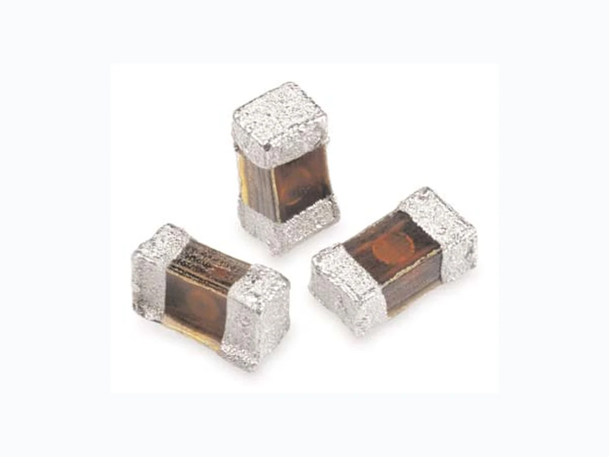
0402ESDA-MLP1 COOPER
Document overview
- Manufacturer or author: Provided By digicamel.com
- PDF pages: 2
Technical content
Features
Halogen free RoHS compliant for global applications Lead free Ultra-low capacitance (0.05pF typ.) ideal for high speed data
applications
Provides ESD protection with fast response time (<1ns) allowing equipment to pass IEC 61000-4-2 level 4 test Single-line, bi-directional device for placement flexibility Low profile 0402/1005 design for board space savings Low leakage current (<0.1nA typ.) reduces power consumption (Sn) Tin-plated version available HALOGEN HFFREE Pb Catalog Number Description 0402ESDA-MLP1 10,000 pieces on paper tape on 7" (178mm) reel - tin plating Specifications Characteristic Value Rated Voltage 30Vdc maximum Clamping Voltage1 35V typical Trigger Voltage2 300V typical Capacitance (@1MHz) 0.05pF typical, 0.15pF maximum Attenuation Change (0-6GHz) -0.2dB typical Leakage Current (@12Vdc) <0.1nA typical ESD Capability IEC61000-4-2 Direct Discharge 8kV typical IEC61000-4-2 Air Discharge 15kV typical ESD Pulse Withstand3 >1000 typical 1 Per IEC61000-4-2, Level 4 waveform (8kV direct, 30A) measured 30ns after initiation of pulse. 2 Trigger measurement made using Transmission Line Pulse (TLP) method.
3 Minor shifting in characteristics may be observed over multiple ESD pulses at very rapid rate
The location in the circuit for the MLP series has to be carefully determined. For better performance, the device should be placed as close to the signal input as possible and ahead of any other component. Due to the high current associated with an ESD event, it is recommended to use a “0-stub” pad design (pad directly on the signal/data line and second pad directly on common ground).
© 2010 Cooper Bussmann www.cooperbussmann.com
1010 BU-SB101153 Page 2 of 2 Data Sheet 4367
The only controlled copy of this Data Sheet is the electronic read-only version located on the Cooper Bussmann Network Drive. Al l other copies of this document are by definition uncontrolled. This bulletin is intended to clearly present comprehensive product data and provide technical information that will help the end user with desig n applications. Cooper Bussmann reserves the right, without notice, to change design or construction of any products and to discontinue or limit distribution of any products. Cooper Bussmann also reserves t he right to change or update, without notice, any technical information con- tained in this bulletin. Once a product has been selected, it should be tested by the user in all possible applications. Life Support Policy: Cooper Bussmann does not authorize the use of any of its products for use in life support devices or system s without the express written approval of an officer of the Company. Life sup- port systems are devices which support or sustain life, and whose failure to perform, when properly used in accordance with instr uctions for use provided in the labeling, can be reasonably expected to result in significant injury to the user. Time (seconds) Temperature (°C) Soldering Recommendations Compatible with lead and lead-free solder reflow processes Peak reflow temperatures and durations: - IR Reflow = 260°C max for 10 sec. max. - Wave Solder = 260°C max. for 10 sec. max. Recommended IR Reflow Profile: Tape and Reel Specifications - mm 10,000 pieces in paper tape on 7 inch (178mm) plastic reel per EIA Standard 481-1 Environmental Specifications Characteristic Value Load Humidity 12Vdc per EIA/IS-772 Para. 4.4.2, +85°C, 85% RH for 1000 hours Thermal Shock EIA/IS-722 Para 4.6, Air-to-Air -55°C to +125°C, 5 cycles Moisture Resistance Test MIL-STD-202G Method 106G, 10 cycles Mechanical Shock EIA/IS-722 Para. 4.9 Vibration EIA/IS-722 Para. 4.10 Resistance to Solvent EIA/IS-722 Para. 4.11 Operating Temperature Range -55°C to +125°C Storage Temperature Range -55°C to +125°C Dimensions - in (mm) 0.021 ± 0.003 (0.530 ± 0.076) 0.014 ± 0.003 (0.360 ± 0.076) 0.043 ± 0.004 (1.100 ± 0.100) 0.010 ± 0.004 (0.250 ± 0.100) 0.016 (0.40) 0.028 (0.70) 0.087 (2.20) Recommended Pad Layout - in (mm) Carrier Dimensions AB DE 1 E2 FG P 1 P2 P3 TW