
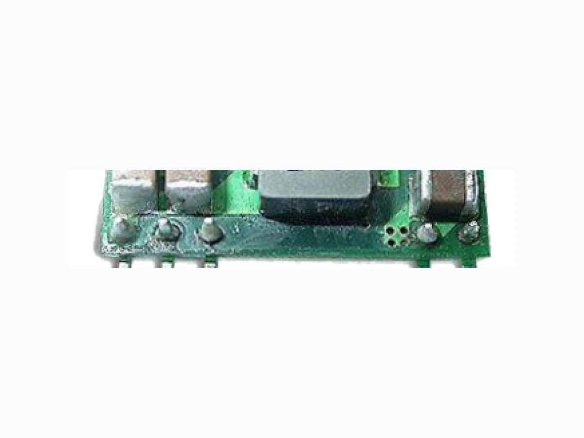
02D-6A YUANDEAN
Document overview
- Manufacturer or author: Provided By www.digicamel.com(FREE DATASHEET DOWNLOAD SITE)
- PDF pages: 4
Technical content
Specifications typical at TA=25°C, nominal input voltage and rated output current unless otherwise specified Part Number ON/OFF Logic Input Range Output Voltage Output Current Efficiency (%) 3.3Vdc @6A Min. Load Max. Load 02D-05-06S Positive (option) Negative (standard) 2.4 ~ 5.5Vdc Vin(min) = Vo(Set)+0.5 0.75 ~3.3Vdc 0A 6A 91% @5.0Vin 02D-12-06S Vo(set)<3.63V Vin=8.3~14Vdc Vo(set)>3.63V Vin=8.3~13.2Vdc 0.75 ~5.0Vdc 93% @12Vin YUAN DEAN SCIENTIFIC YUAN DEAN SCIENTIFIC CO.,LTD Rev:0 2018/10/31
02 D-6A SERIES
Parameters Conditions Min Typ Max Units Voltage Tolerance
05 Series
Vo(set) 2.4 5 5.5 Vdc
12 Series
Vo(set) 8.3 12 14 Input Current Vin=Vin(min); Io=Io(max) 6 A Input Filter(Note4) C filter No Load Current Vo(set)=0.75Vdc 20 @Vin=5 mA Vo(set)=0.75Vdc 19 @Vin=12 mA Vo(set)=3.3Vdc 45 @Vin=5 mA Vo(set)=5.0Vdc 100 @Vin=12 mA Under Voltage Lockout Start-up Voltage 2.2@Vin= 5 V 4.5@Vin=12 Shutdown Voltage 2.0 @Vin=5 V 3.8 @Vin=12 Input reflected ripple current 5~20MHz, 1uH source impedance:35mAp-p Applicati ons Wireless Network Telecom/Datacom Distributed Power Architectures Industry Control System Semiconductor Equipment Microprocessor Power Applications FEATURES : SIP Packages High Efficiency 9 1% @5.0Vin 3.3V ,Full Load 93% @12.0Vin 3.3V ,Full Load Customized Solutions Available Operating Temperature From -40℃ To +85℃
3 Years Warranty
Input Under-Voltage Lockout Input Range 2.4VDC To 5.5VDC, 8.3VDC To 14VDC Output Current Up To 6A Output Voltage Programmable From 0.75VDC To 3.3VDC, 0.75VDC To 5VDC Via External Resistor
Parameters Conditions Min Typ Max Units Switching Frequency 300 KHz Isolation voltage None Efficiency See table Dimensions As figure of marking and dimension mm Weight 2.8 g MTBF (Note 1) MIL-HDBK-217F 3.247 x 10 6 Hours 02D -12 -06 S,Vo=3.3V,Derating Cu rve 02D -05 -06 S,Vo=3.3V Efficiency VS Input Voltage YUAN DEAN SCIENTIFIC CO.,LTD Rev:0 2018/10/31 02D -05 -06 S,Vo=3.3V,Derating Curve 02D -12 -06 S,Vo=3.3V Efficiency VS Input Voltage Output Specifications Parameters Conditions Min Typ Max Units Output current 6 A Voltage Tolerance Full load and Vin(min) ±2 % Minimum load 0 A Line Regulation Vin=Vin ( min ) to Vin ( max ) at Full Load ±0.3 % Load Regulation No Load to Full Load ±0.5 % Ripple & Noise (Note2) 20MHz bandwidth 60 mVp-p Dynamic load response (Note 2) ΔIo /Δt = 2.5A/uS ,Vin(nom) Peak deviation 200 mV Load change step (25% to 100% or 100% to 25% of Io(max)) Setting time (Vo<10%peak deviation) 25 uS Dynamic load Response (Note 3) ΔIo /Δt = 2.5A/uS ,Vin(nom) Peak deviation 50 mV Load change step (25% to 100% or 100% to 25% of Io(max)) Setting time (Vo<10%peak deviation) 50 uS Output current limit 220 % Output short- circuit current Hiccup, automatic recovery External load capacitance ESR ≧1mΩ 1000 uF ESR ≧10mΩ 3000 uF Output voltage overshoot- startup Vin=Vin(min) to Vin(max);F.L 1 % Voltage adjustability (see fig.1) 05 Series 0.7525 3.3 @Vin=5 V 12 Series 0.7525 5.0 @Vin=12 V
02D -05 -06 S,Vo=3.3V Efficiency VS Output Load 02D -12 -06 S,Vo=3.3V Efficiency VS Output Load 02 D-6A SERIES YUAN DEAN SCIENTIFIC CO.,LTD Environmental Specifications Parameters Conditions Min Typ Max Units Operating temperature range with derating -40 85 ℃ Storage temperature range With derating -55 125 ℃ Thermal shock MIL-STD-810F Over temperature protection 135 ℃ Feature Specifications Parameters Conditions Min Typ Max Units Remote ON/OFF Positive logic(option) ON=(Vin-4)<Vr<Vin(Max) 10 uA OFF=0V<Vr<0.3V 1 mA Negative logic(standard) ON=0V<Vr<0.3V@IIN 10 uA OFF=1.5V<Vr<Vin(Max)@IIN 1 mA Input current of Remote control pin 0.01 1.0 mA Remote off state input current Nominal Vin 5 mA Rise time (Time for Vo to rise from 10% to 90%of Vo(set )) 6 ms Turn-on delay time Case 1 (Note 5) ms Case 2 (Note 6) 3 ms Note : 1. MIL-HDBK-217F Notice2 @Ta=25 ºC, Full load(Ground, Benign, controlled environment). 2. External with Cout = 1uF ceramic//10uF tantalum capacitors. 3. External with Cout = 2×150uF polymer capacitors. 4. It’s necessary to equip the external input capacitors at the input of the module. The capacitors should connect as close as possible to the input terminals that ensuring module stability. The external Cin is 2×150μF low- ESR polymer capacitors // 2×47μF ceramic capacitors at least. 5. Case 1 :On/Off input is set to logic low (module on) and then input power is applied (delay from instant at which Vin=Vin(min) until Vo=10% of Vo(set)) 6. Case 2 :Input power is applied for at least one second and then the On/Off input is set to logic low (delay from instant at which Von/off=0.3V until Vo=10% of Vo(set)) CAUTION: This power module is not internally fused. An input line fuse must always be used. Rev:0 2018/10/31
Rev:0 2018/10/31 02 D-6A SERIES YUAN DEAN SCIENTIFIC CO.,LTD Dimensions PIN Assignment Pin 1 2 3 4 5 Function +Vout Trim GND +Vin Remote On/Off